Products Page
FTDI Dual Channel Serial Ports
Richard, you will enter the product info here and it will be displayed.
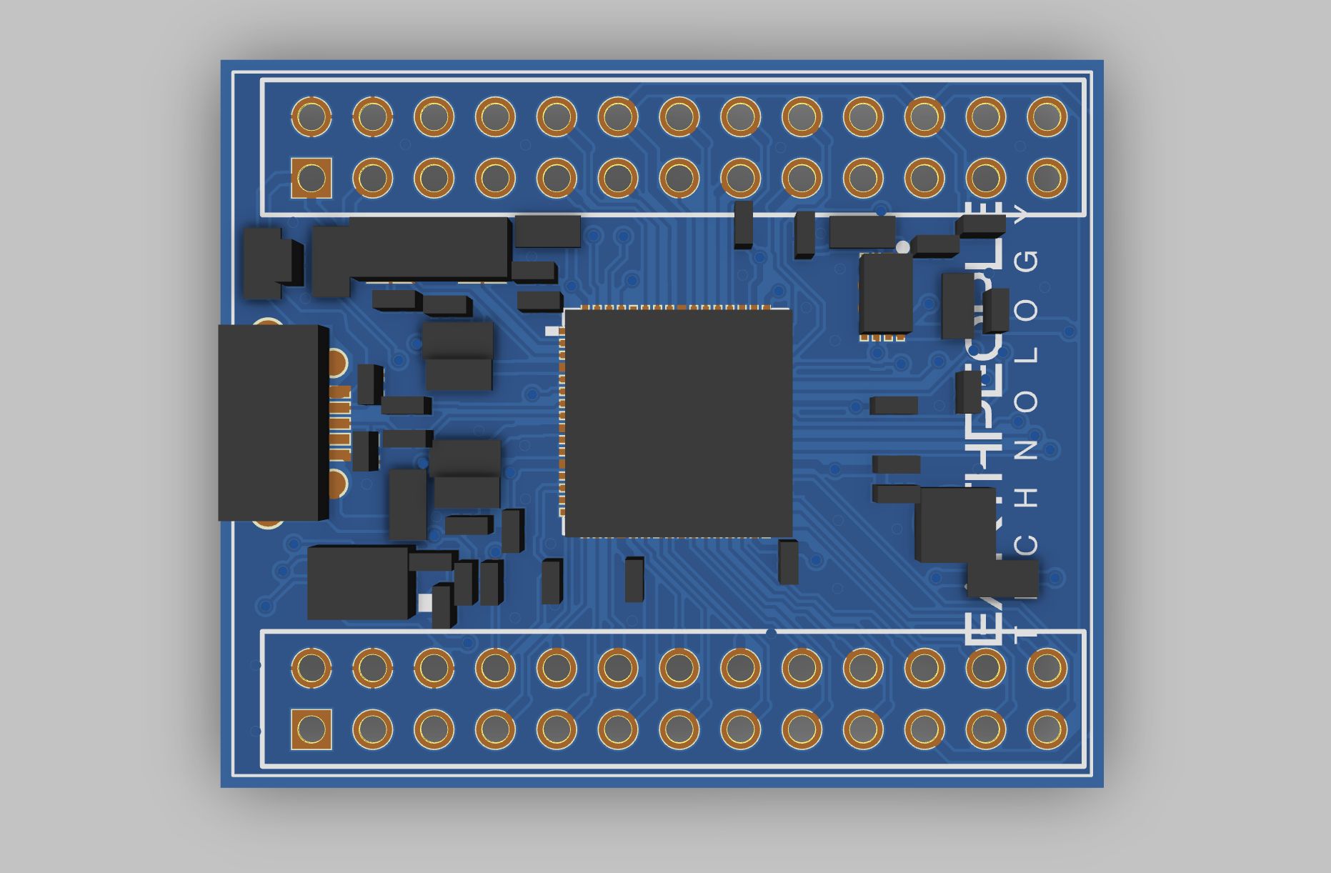
EPT-2232-MM-D2-1
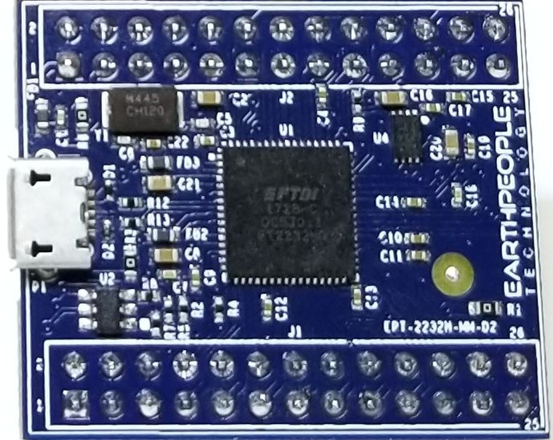
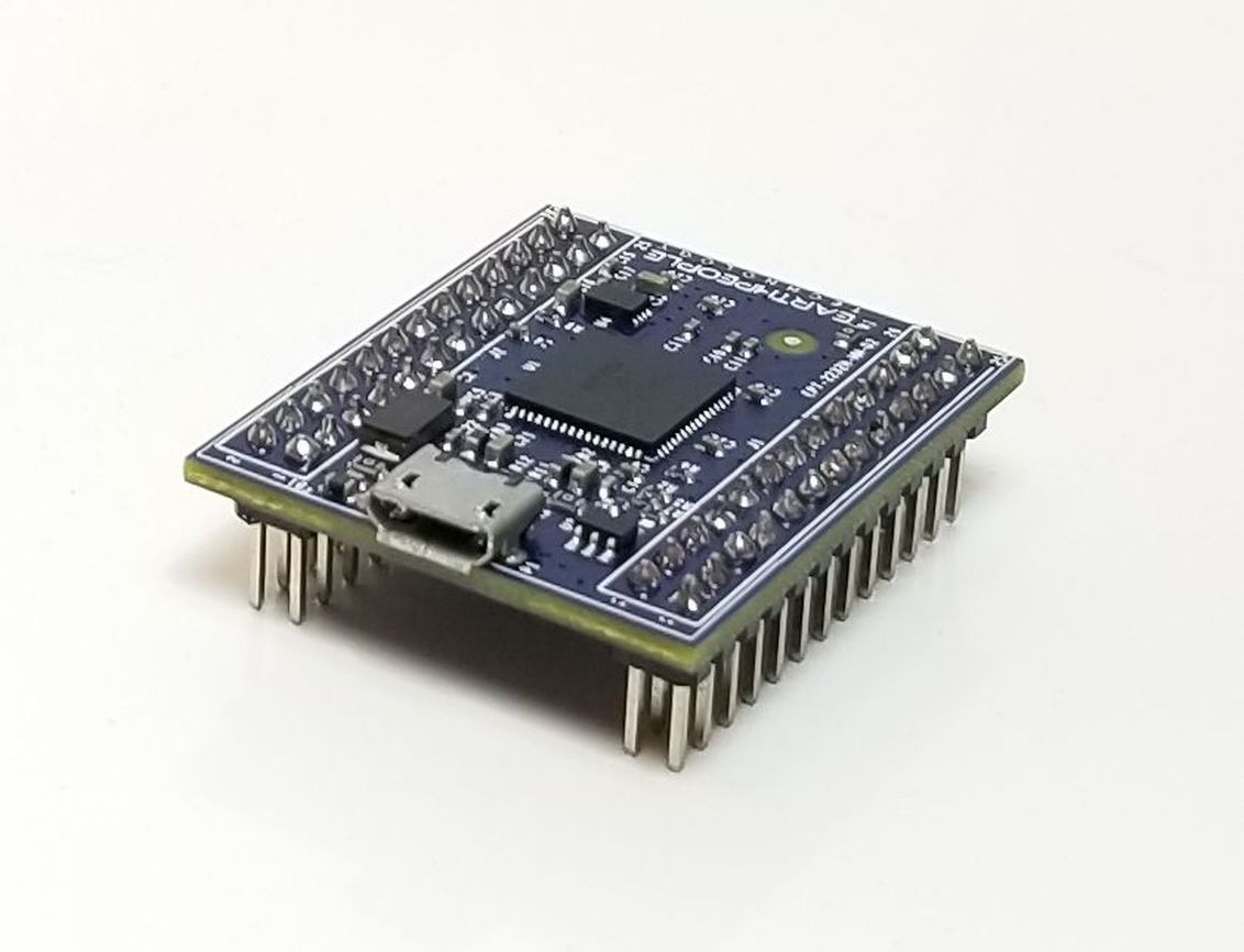 Dual Channel FTDI Breakout Board
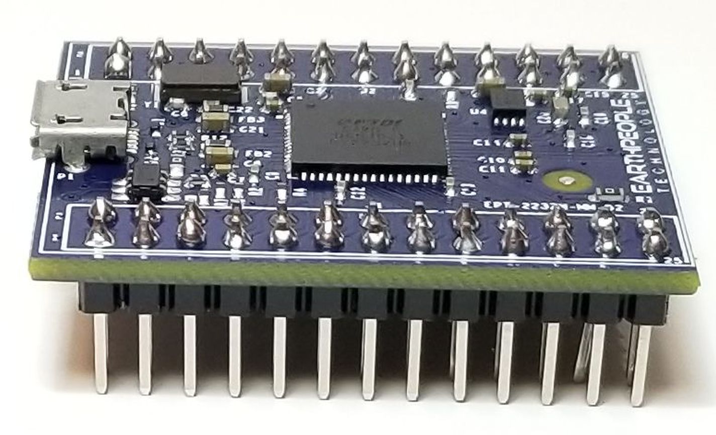
SPECIAL ORDER
30 PIECES OF FTDI BREAKOUT BOARD
TOTAL $599.70
FREE SHIPPING
NO FEES
|
This breakout board is based on the FTDI FT2232H USB 2.0 IO chip. The FT2232H |
|
The FT2232H Breakout Board contains the MPSEE engine. This engine can output SPI, I2C, JTAG or act like an eight bit parallel port. Using the JTAG interface, the FTDI Breakout Board can program the ATMega and Arduinos. It is supported by OpenOCD, urJTAG and others. Hardware Features: |
|
 |
|
The breakout board includes an external EEPROM for custom USB descriptors and VID/PIDs, Serial Numbers, Driver selection (Virtual COM Port or D2XX drivers). There are two 13×2 Headers on 0.1 inch pitch installed on the bottom of the board. An external +3.3V LDO provides power for the FT2232H chip as well as powering off board electronics. The FT2232H chip can operate up to 12MBaud data transfer rates via USB 2.0. It features the USB Micro-B connector. |
Downloads
| 85-000001 | Dual Channel FTDI Breakout Board User Manual | DUAL_CH_FTDI_BREAKOUT_UM.pdf |
| 95-000001 | Dual Channel FTDI Breakout Board DataSheet | DUAL_CH_FTDI_BREAKOUT_DS.pdf |
| 55-000001 | Dual Channel FTDI Breakout Board Schematics | DUAL_CH_FTDI_BREAKOUT_SCHEMATIC.PDF |
| 35-000001 | EPT Drivers | EPT_2.12.00.exe |
EPT-2232H-SP-S1
 JTAG Blaster
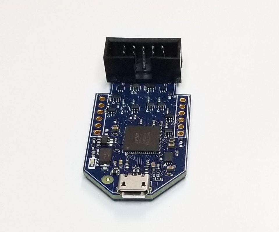
Altera JTAG Blaster Provides JTAG connectivity for Altera devices only |
|
It is designed to program CPLDs and FPGAs from Altera only. It allows JTAG connectivity of any target device voltage from +1.2V to +5V. The Altera JTAG Blaster is compatible with Windows PCs Only. It is not compatible with Linux. |
Program CPLDs and FPGAs
|
The driver provided by Earth People Technology allows this board to be used by the Quartus Application Programmer. Once this driver has been successfully installed, the device can be found in the Hardware Setup drop down box. Just select the device and the programming mode and the appropriate programming file and the board will program your device. |
|
This device connects to an open USB port on a Windows PC and allows the Quartus Programmer application to directly program Altera devices. Installation of the EPT-JTAG- Blaster Driver is required for this device. |
Specifications:
|
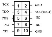
| The 5×2 connector has the same pinout as Altera Blasters. |


Downloads
| 85-000012 | EPT JTAG Blaster User Manual | EPT_JTAG_BLASTER_UM.pdf |
| 95-000013 | EPT JTAG Blaster Data Sheet | ALTERA_JTAG_BLASTER_DS.pdf |
| 45-000013 | EPT JTAG Blaster Project DVD | JTAG_BLASTER_GETTING_STARTED_GUIDE.pdf |
| 55-000013 | EPT JTAG Blaster Schematics | EPT_2232H_SP_S1_V2_SCH.pdf |
| 35-000013 | EPT JTAG Blaster Driver | jtag_hw_mbftdi_blaster64.dll |
| 35-000100 | EPT Drivers | CDM212365_SETUP.ZIP |
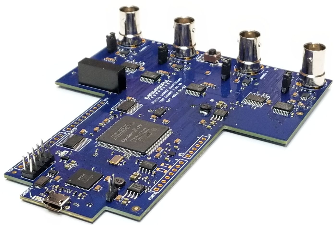
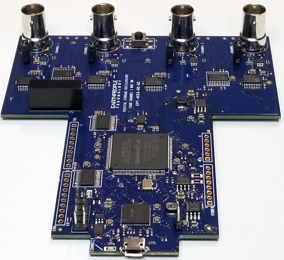
DueProLogic USB-FPGA Development System
ALTERA
CYLONE IV FPGA
DEVELOPMENT
SYSTEM
The DueProLogic is a complete FPGA
Development System designed to easily
get the user started learning and
creating projects.
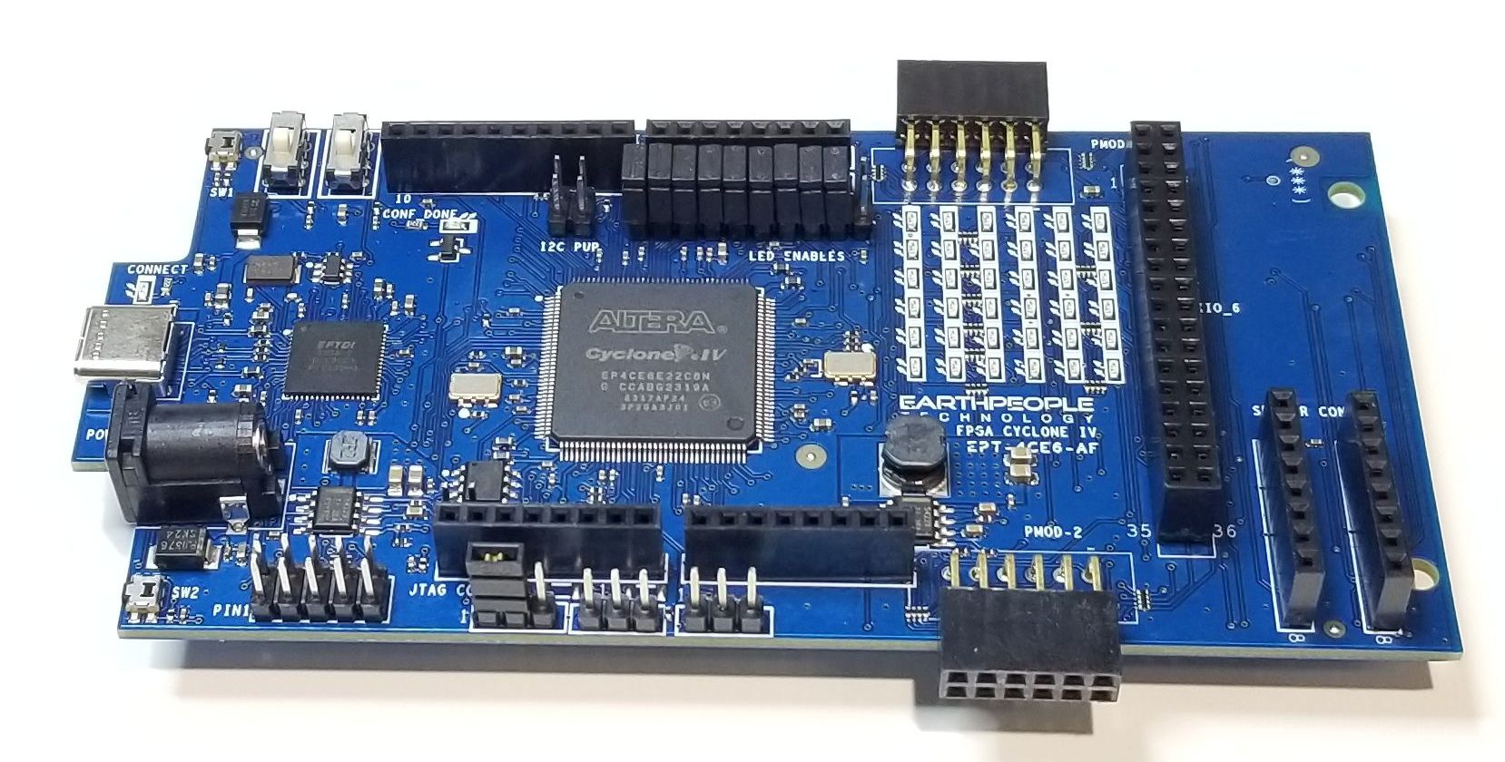
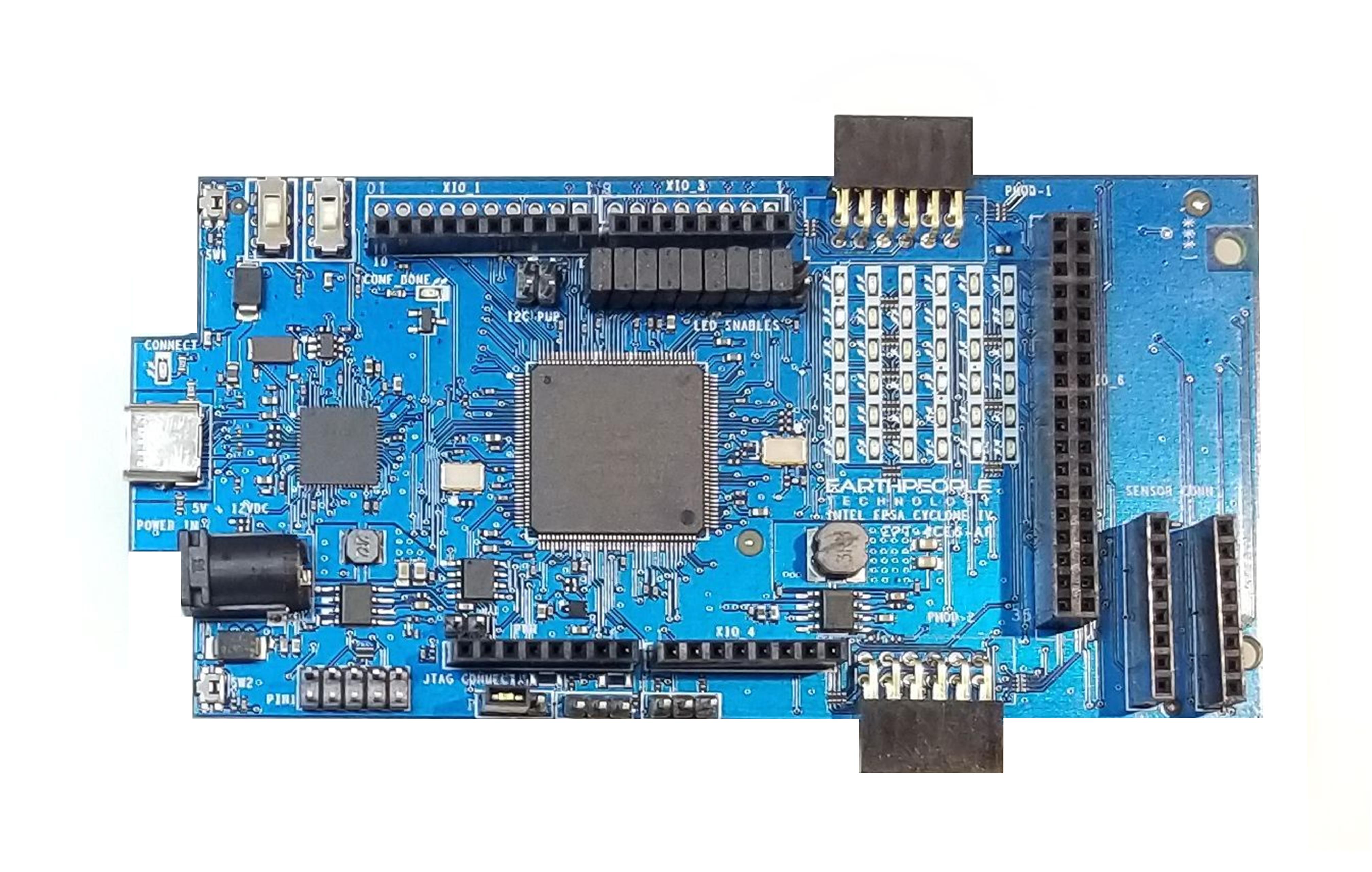
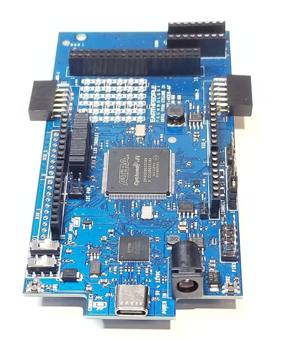
| The DueProLogic makes programmable logic easy with an all inclusive development platform. It includes an Intel/Altera Cyclone IV FPGA, on board programming, four megabit configuration flash, and an SD connector for add on memory. You can create your HDL code, program it into the flash and interact with the hardware via a Windows PC. |
| This is the FPGA (Field-Programmable Gate Array) development board and runtime environment you have been waiting for to get started with programmable logic. |
DueProLogic FPGA Development System
| The DueProLogic (DPL) and its integrated development and distinctive runtime environment has been specifically designed for Electrical Engineering students, hobbyists, and entrepreneurs prototyping/developing/running projects involving logic, with the added opportunity, should it be needed for your project, of readily mating with a widely used microprocessor board, the Arduino Due, and other ARM Cortex compatibles. The combination of FPGA programmable logic and microcontroller is unbeatable in an educational student learning setting and in many other projects where each can bring its strength. |
FPGA Training
| The DPL gives learners the opportunity to have an appropriate hands-on approach when learning logic, exploring different iterations of schematic/code designs with simple uploads of the design, and the operation of those circuits with relatively easy runtime passing of project parameters and data, and an abundance of headers that can interface to external components, without having to spend inordinate amounts of time reading datasheets, designing the right combinations of gates on multi-gate chips, and building/revising/debugging/revising repeatedly… spaghetti bowls of wires and chips on multiple breadboards to connect to those same external components. With the DPL’s FPGA, projects can also more easily be attempted which rely on asynchronous, exceedingly fast, and even multiple separate concurrent logic structures operating in parallel which would have traditionally required a plethora of chip gates or multiple high speed microprocessors to implement parallel processes. Logic circuits are implemented within the FPGA at few- nanosecond gate speeds and highly parallel in operation, effectively a few hundred MHz; Microprocessors often rely on inherently slower single threaded program loops with interrupt servicing, which is typically much slower. Programmable logic is today’s technology for logic learners and implementers, replacing discrete logic chips. |
FPGA Projects
| The DPL allows the learner to be more productive and better focus on the underlying logic and integration with the non-logic aspects of non-trivial projects. Projects and solving real-world applications might involve: |
|
DueProLogic Overview
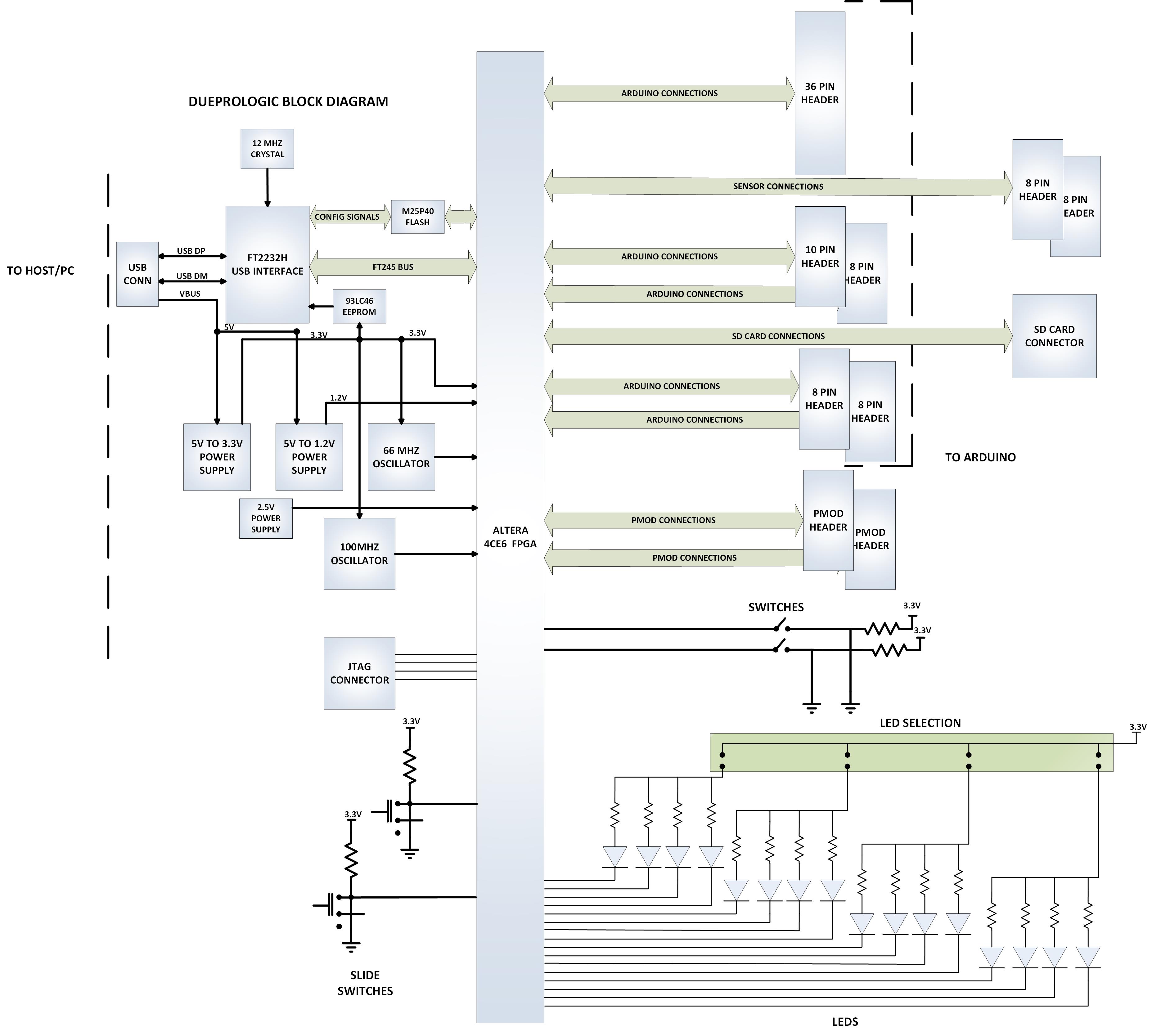
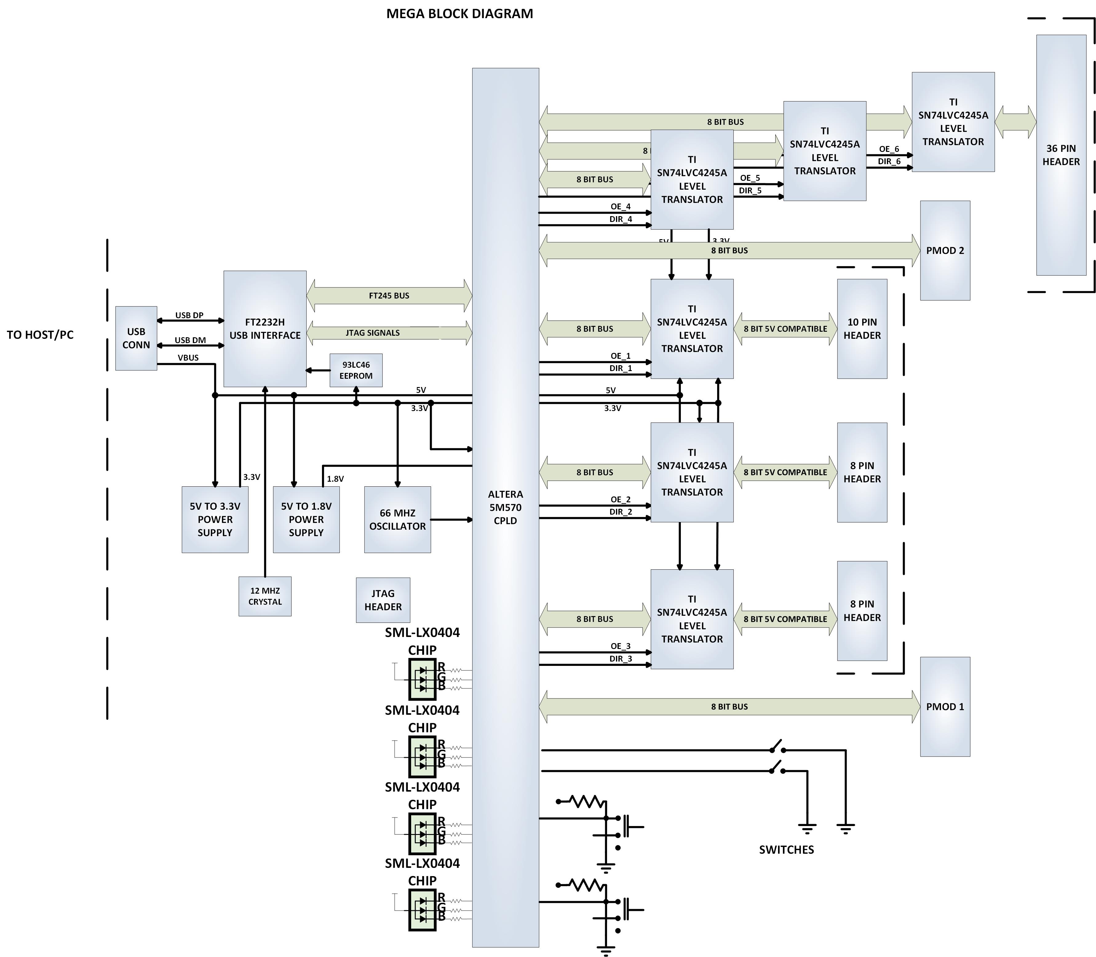
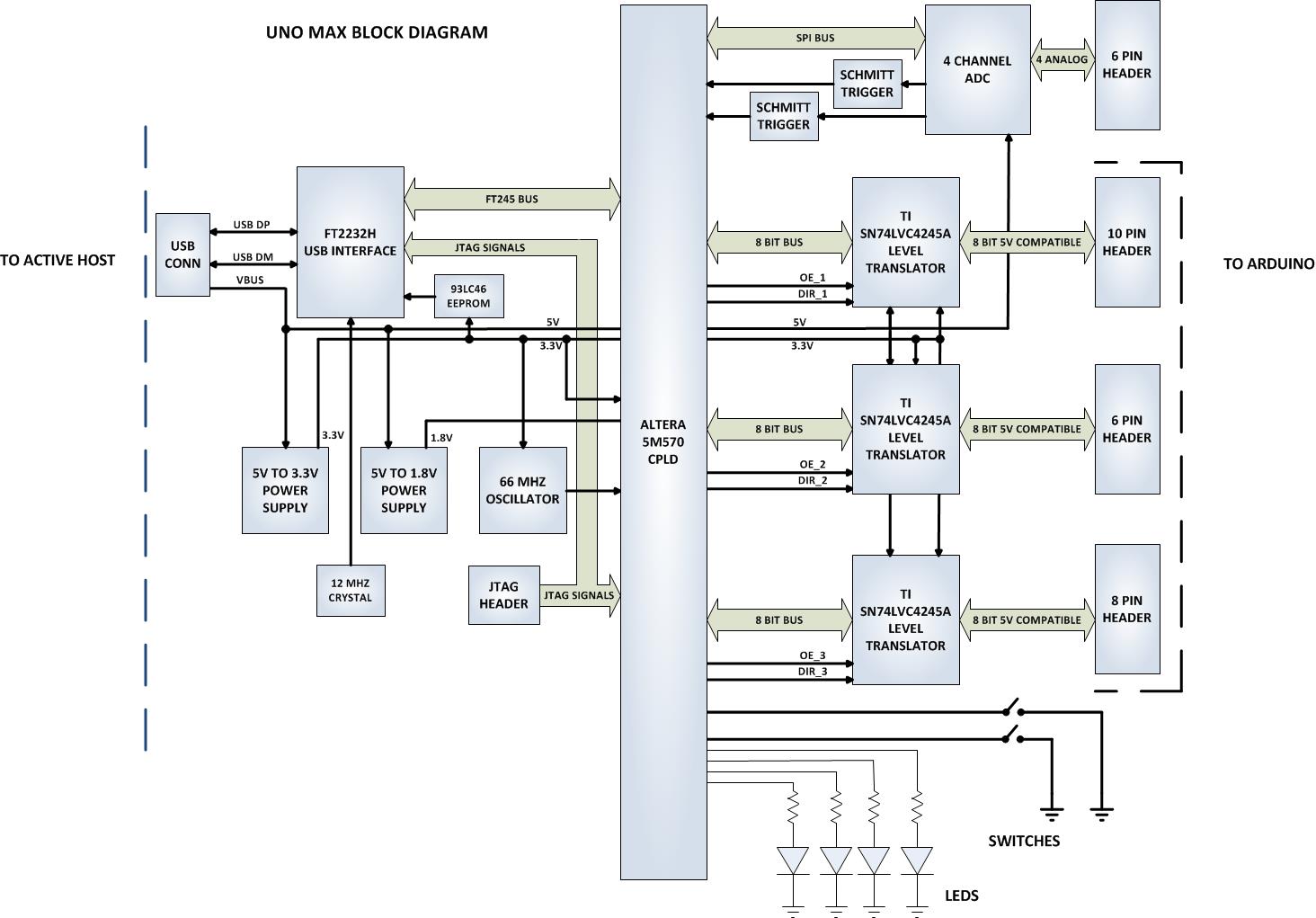
| The DPL is a complete FPGA development environment. It includes a powerful Intel/Altera Cyclone IV FPGA, High-Speed USB interface chip, Full SD Card interface connector, and 4Mb Configuration Flash (for the FPGA). The USB interface chip is an FT2232H with Dual Serial Channels. One channel is dedicated to loading the configuration Flash for the FPGA. The second channel provides a high speed interface for bi-directional communications with the FPGA. Once the configuration Flash is loaded with the users synthesized code, a reset will cause the FPGA to read the Flash and load up the stored image into the FPGA. |
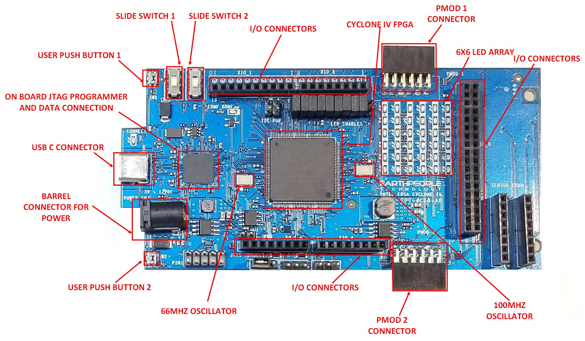
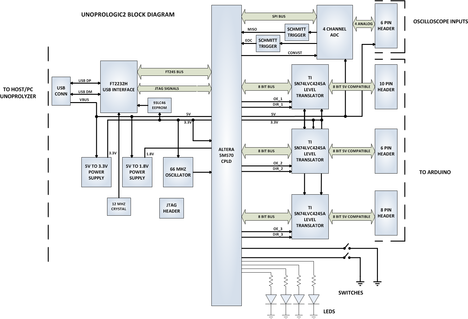
| The block diagram shows all of the parts of the DueProLogic. There are two main power supplies, +1.2V and +3.3V. The +1.2V powers the core of the FPGA while the +3.3V powers the Input/Outputs of the FPGA as well as provides power for user circuits. The DPL contains two oscillators, 66MHz and 100MHz. The 66MHz oscillator is used to provide clocking for the EPT ActiveHost USB communications core. The 100MHz oscillator can be used by the user clocked up using one of the onboard Clock-DLL modules. |
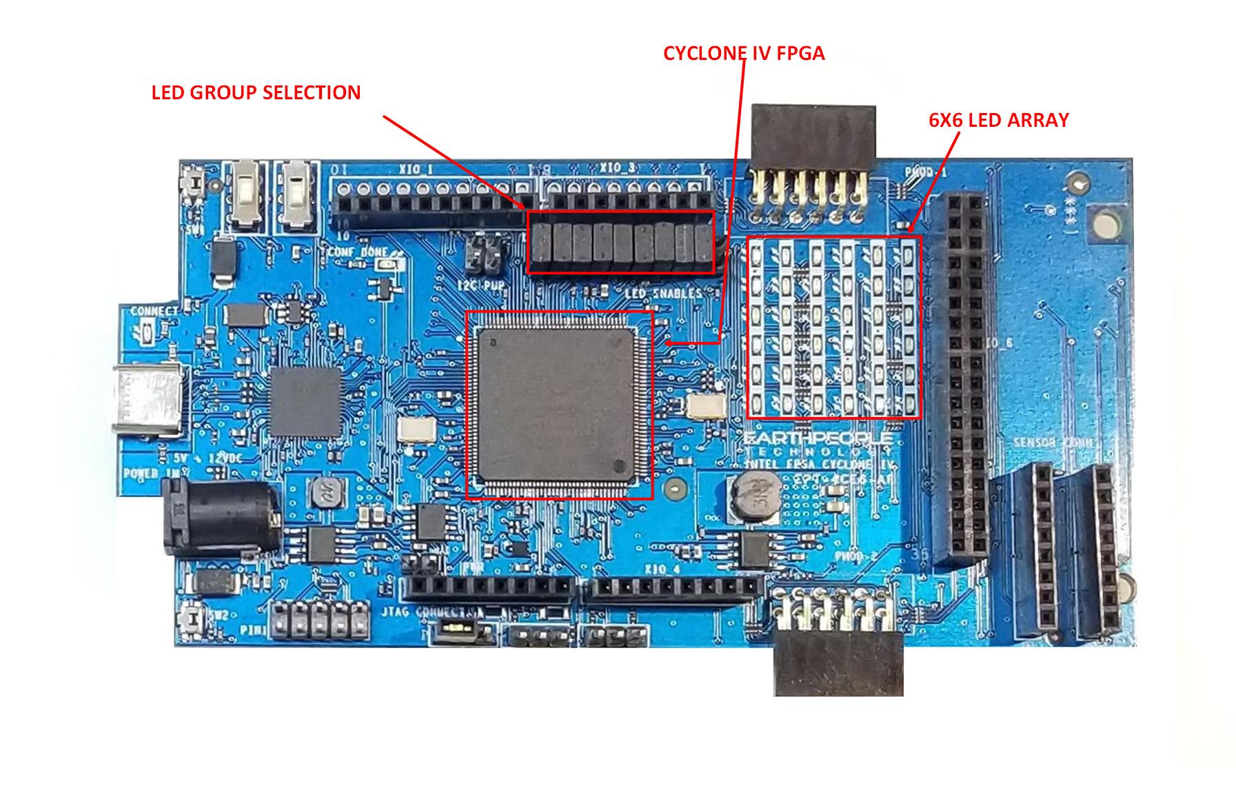
6×6 LED Array
Development Environment
| The DueProLogic includes a 6×6 Green LED array. Each LED is sinked to an individual pin on the FPGA. Each LED is current limited to 6mA. The total current consumed for all 36 LEDs is 216mAs. The FPGA can easily sink this current. So, individually sinking all 36 LEDs makes easy control for User Code. The DueProLogic also contains a method to turn on/off the LEDs in four unit blocks. A jumper is used to control the state of each LED block. |
DueProLogic Block Diagram
Development Environment
| The DPL User Manual comes complete with instructions to set up all the drivers, the Intel/Altera Quartus development environment, and get started creating FPGA projects. The User Manual walks the user step by step from start to finish of the first FPGA project. |
| The included Windows development environment kit includes: Quartus Prime Lite for compiling user code, assigning pins, project setup, programming and other items. The kit also includes the EPT ActiveHost core for the DPL, to facilitate communication between the PC and DPL while the DPL is running a developed project. The kit also EPT has developed a .dll that allows Quartus Prime Lite to directly program the DPL in the same way USB-Blaster works with other Intel/Altera populated development boards. |
|
Configuring the FPGA
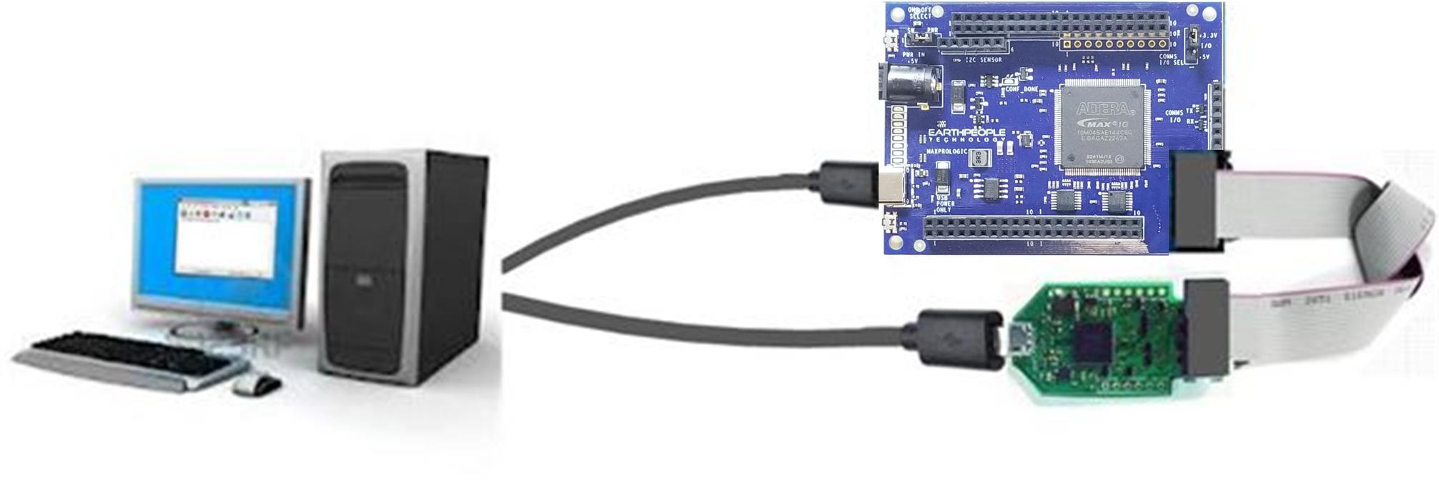
| The FPGA on the DPL can be programmed with the HDL project created by the user. Configuration is quick and easy. All that is required is a standard USB cable with a Micro Type B connector, and the EPT Blaster Driver DLL installed on the PC. There are no extra parts to buy – just plug in the USB cable and connect the DueProLogic to the PC. |
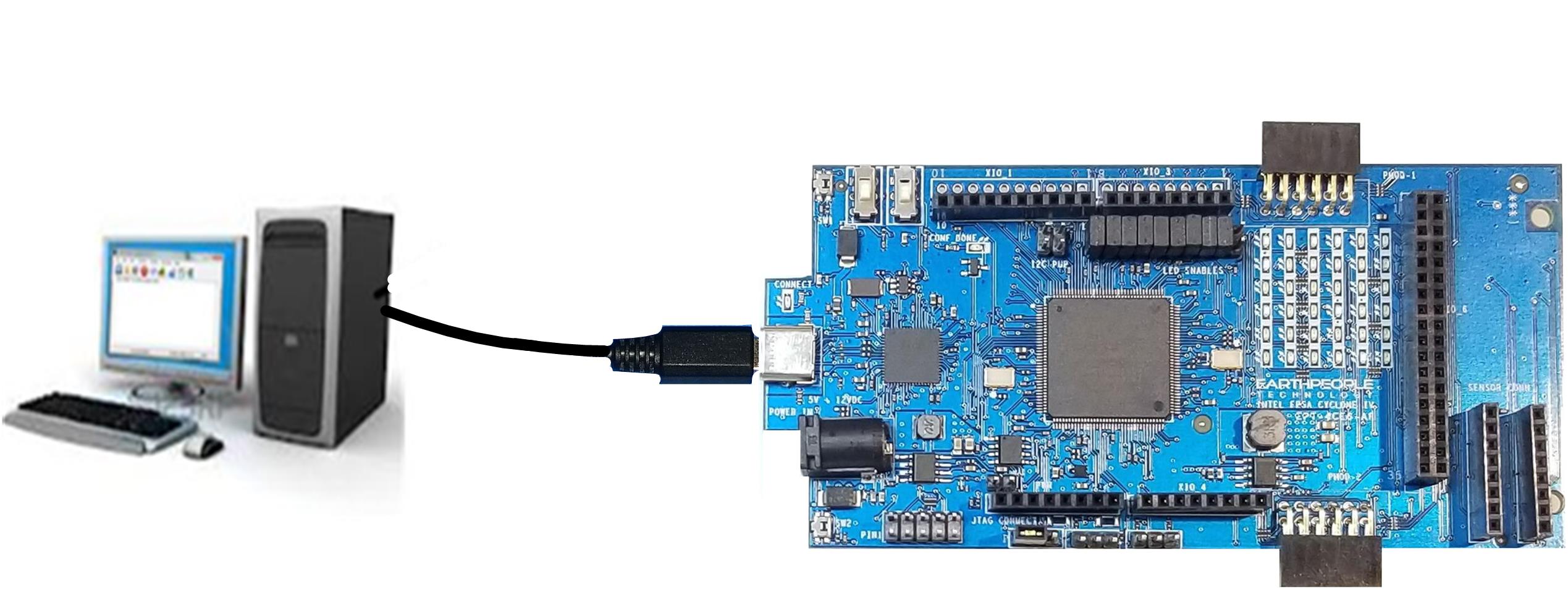
| The DPL Configuration Flash is programmed using the Quartus development environment and the EPT Blaster Driver. Once the the Configuration Flash is programmed. A reset will cause the FPGA to begin configuring itself using the Flash. |
| The board comes preloaded with Blinky, the test that each board goes through before being shipped with conductive foam in a static-control bag. Also included with the product is a DVD with the needed PC/Quartus/DPL drivers, library, User Manual, Schematics, and sample projects, which are also available on the EPT web site. To save expense and possibly the environment, and because many purchasers already have a micro-USB data cable, one is not included. |
| Specifications: Designed to be stand-alone and/or be mated with an Arduino Due. Designed to be inserted directly into a standard breadboard, for easier prototyping Designed with the Arduino Due shield header layout, to accommodate 3.3v-compatible Arduino-type shields, plug-in modules EPT offers, or modules you might develop using standard 0.1” pitch single or double row pin headers. Designed and assembled in the USA and made to be RoHS (no Lead) compliant around the world. The DPL is made to accept standard USB Micro B cable connection and power input of 5-15VDC, but the header logic pins are only 3.3V compatible, like most other high-speed products using today’s chips. Applying 5V to a pin connected to the FPGA chip will cause permanent damage to the FPGA chip. |
DueProLogic Features:
|
Downloads
| 85-000012 | DueProLogic FPGA Development System User Manual | DPL_FPGA_DEV_SYS_UM.pdf |
| 95-000012 | DueProLogic FPGA Development System Data Sheet | DPL_FPGA_DEV_SYS_DS.pdf |
| 45-000012 | DueProLogic FPGA Development System Project DVD | DUEPROLOGIC FPGA PROJECT DVD |
| 55-000012 | DueProLogic FPGA Development System Schematics | EPT-DPL-USB-FPGA-SCHEMATICS.pdf |
| 35-000001 | EPT Drivers | EPT_2.08.24.ZIP |
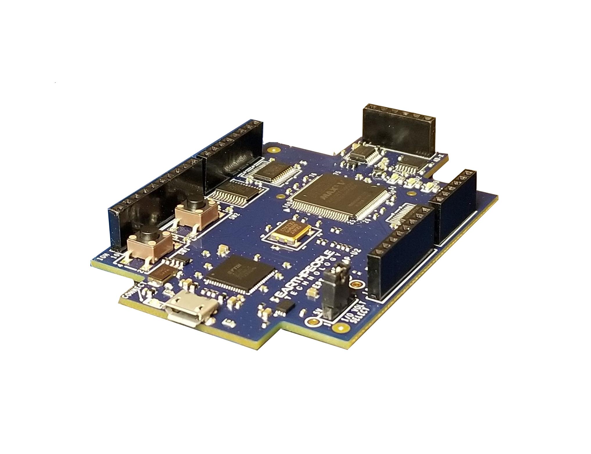
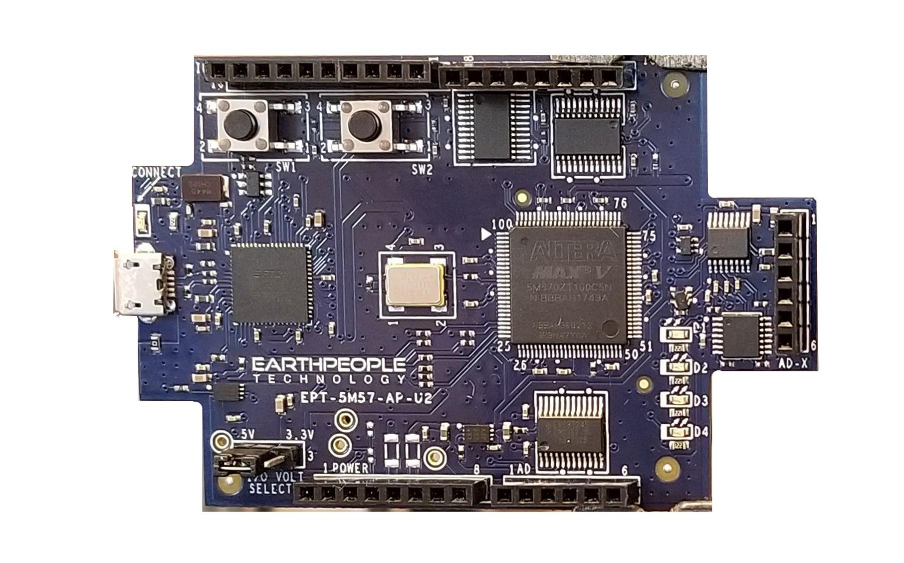
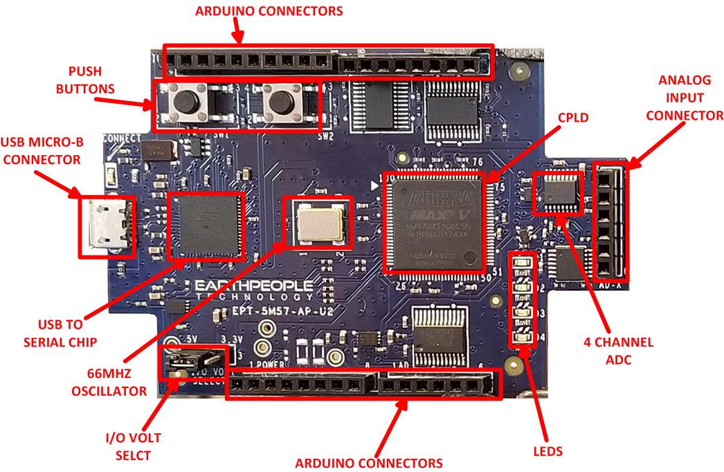
UnoMax CPLD Development System

The UnoMax is an easy to use
CPLD development system. It includes
a four Channel ADC and built in
programmer
Purchase at these webstores:
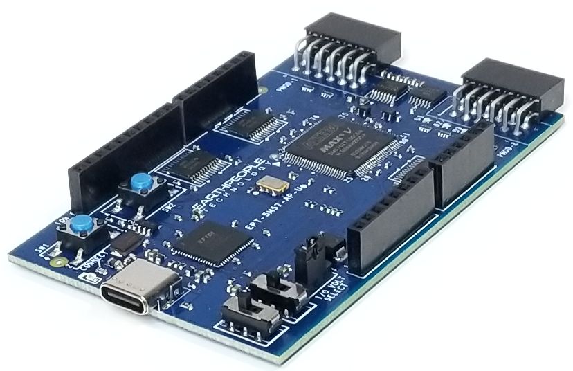
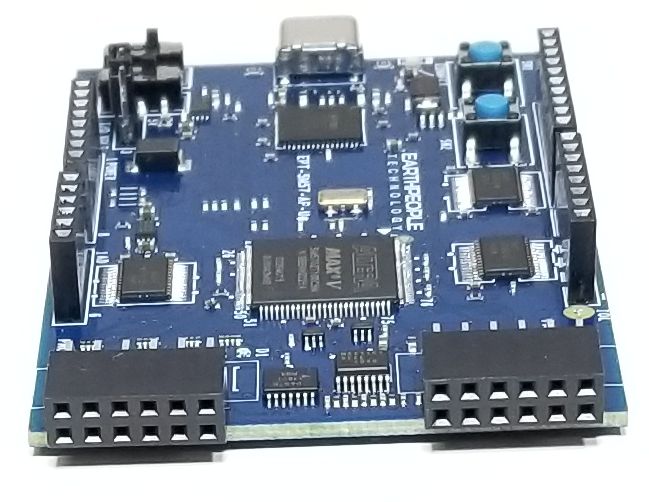
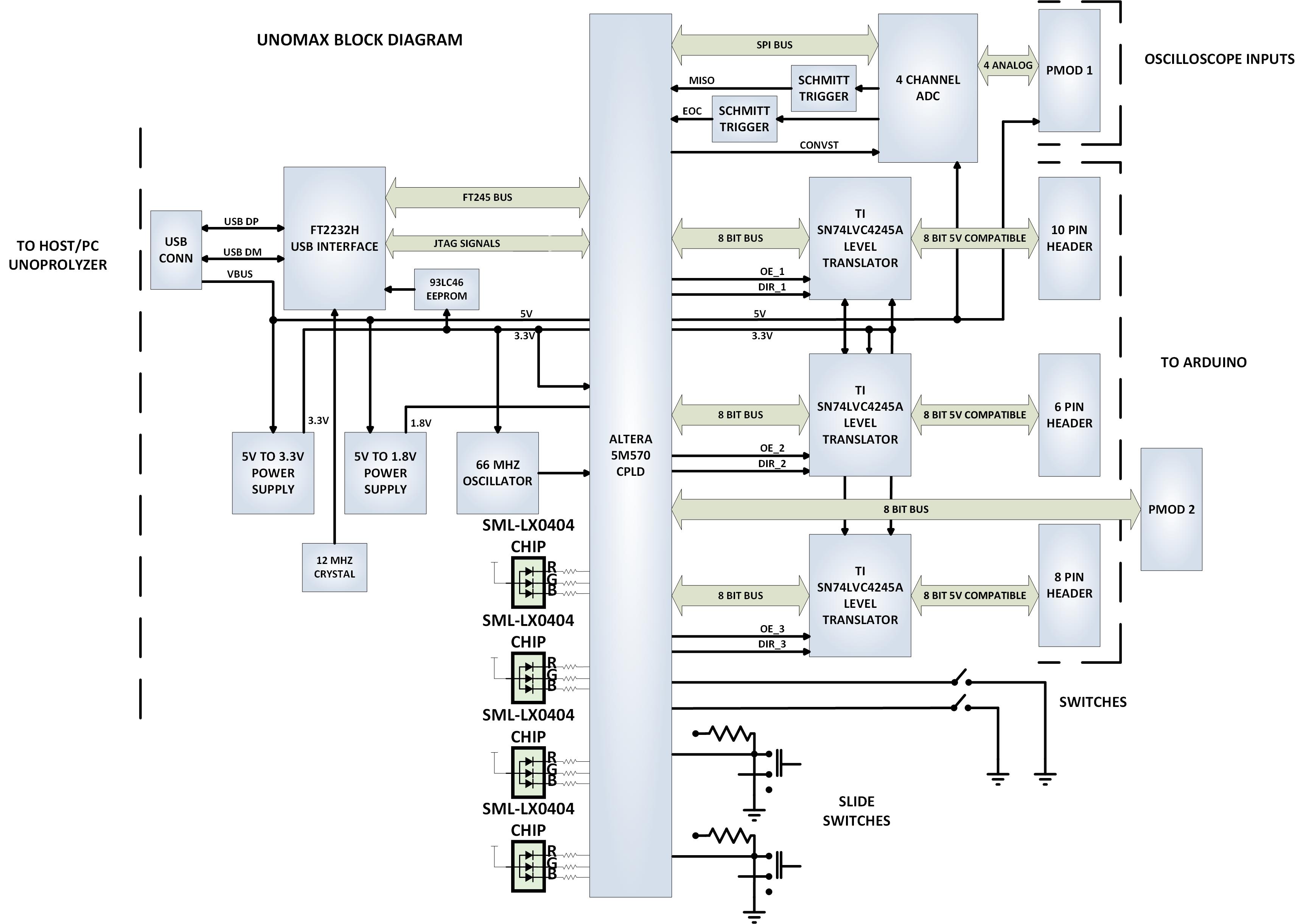
| The UnoMax makes programmable logic easy with an all inclusive development platform. It includes an Intel 5M570 CPLD, JTAG programmer, and a four channel ADC with 300KS/second sample rate. You can create your HDL code, program it into the CPLD and interact with the hardware via a Windows PC. |
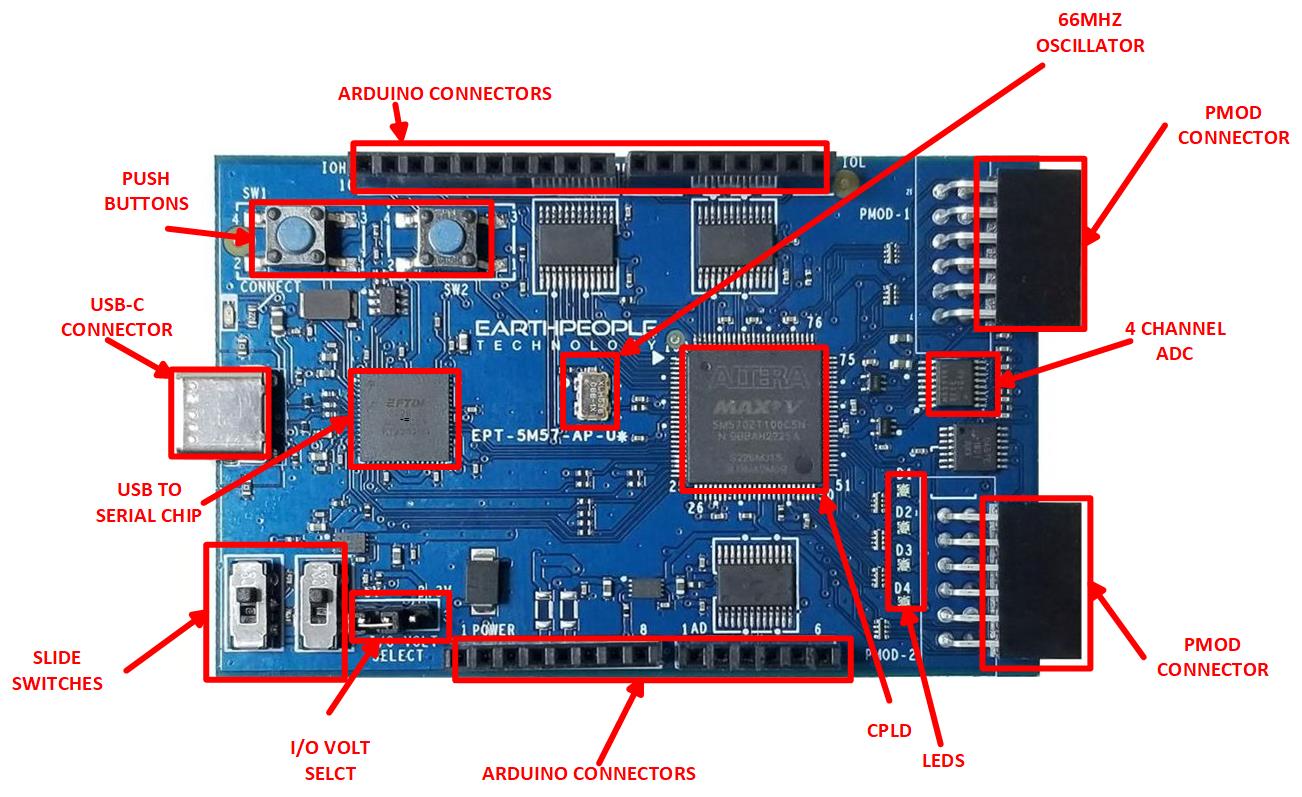
| The UnoMax is designed as a single board solution for developing programmable logic circuits. It includes robust power supplies that run from a single USB connection from the PC. 24 Input/Outputs are available at board edge connectors and PMOD connectors. The board edge connectors provide protection from over voltage/current by using bus transceivers. These transceivers prevent the user from connecting external signals directly to the CPLD. |
Hardware Features:
|
| The UnoMax DVD provides detailed step by step instructions to quickly guide the user to create a project,. synthesize the project and download the programming file into the CPLD. The Quartus Prime Software must be downloaded from Intels website. Once the Quartus software is on your desktop, the guide will show you how to create a project, write you first LED blinky code, compile and program the CPLD. |
|

Programming the CPLD
| The CPLD on the UnoMax can be programmed with the code created by the user. Programming is quick and easy. All that is required is a standard USB-C cable and the Quartus Software installed on the PC. There are no extra parts to buy – just plug in the USB cable and connect the UnoMax to the PC. |
![]()

Connecting To Hobby Electronics Made Easy
| The UnoMax easily connects to other Hobby Electronics. The durable 74LVC82245 Bus Transceivers allow up to 50mA per Output on the Stackable Headers. This kind of power can drive all kinds of electronics such as long distance cables, LEDs, and high speed electronics. |
Programmable Logic Code Development
| It also provides a high speed data transfer mechanism between the UnoMax board and a host PC. The UnoMax development system provides a convenient, user-friendly work flow by connecting seamlessly with Altera’s Quartus Prime Lite software. The user will develop the code in the Quartus environment on a Windows Personal Computer. The programmable logic code is loaded into the CPLD using only the Quartus Programmer tool and a standard USB cable. The Active Host SDK provides a highly configurable communications interface between CPLD and host. It connects transparently with the Active Transfer Library in the CPLD code. This Active Host/Active Transfer combination eliminates the complexity of designing a USB communication system. No scheduling USB transfers, USB driver interface or inf file changes are needed. The UnoMax development systemis a unique combination of hardware and software. |
| Use the C# examples included in the DVD to create your own display Window on the PC.The user comes complete with tutorial to instruct the user to easily build a Windows program that can display any data from user code or other electronic device. The C# interface uses similar function calls to the Arduino function calls. |
4 Channel Analog to Digital Converter
| Examine four analog channels running up to 300 KSamples/second. The hardware has been simplified to remove extra cost.The input signals are limited to 0 to +5Volts and the sample rate is shared across all four channels. If you run one channel only, it will take advantage of the 300KSamples/second. If you run four channels, each channel will have a maximum sample rate of 75 KSamples/second. |
![]()
Programming Features:
|
Kit Contents
| UnoMax kit contains the UnoMax and a DVD which includes the User Manual that walks the user through setting up the drivers, software, how to use to the test application. There is also a full tutorial in writing yourfirst CPLD project and C# application. All the code for the projects are included. |
Downloads
| 85-000040 | UnoMax CPLD Development System User Manual | UNOMAX_CPLD_DEV_SYS_UM.pdf |
| 95-000040 | UnoMax CPLD Development System Data Sheet | UNOMAX_CPLD_SYS_DS.pdf |
| 45-000040 | UnoMax CPLD Development System Project DVD | UNOMAX_CPLD_SYSTEM_PROJECT_4.5_DVD |
| 55-000040 | UnoMax CPLD Development System Schematics | UNOMAX_SCHEMATICS.PDF |
| 35-000001 | EPT Drivers | CDM212364_Setup.ZIP |
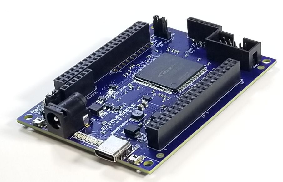
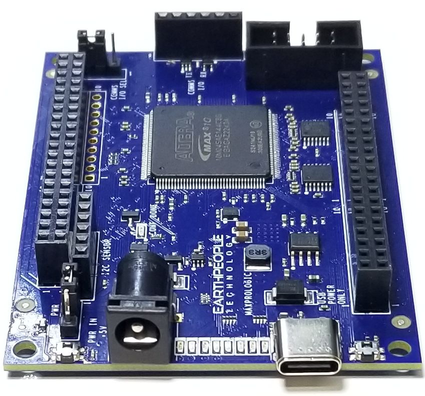
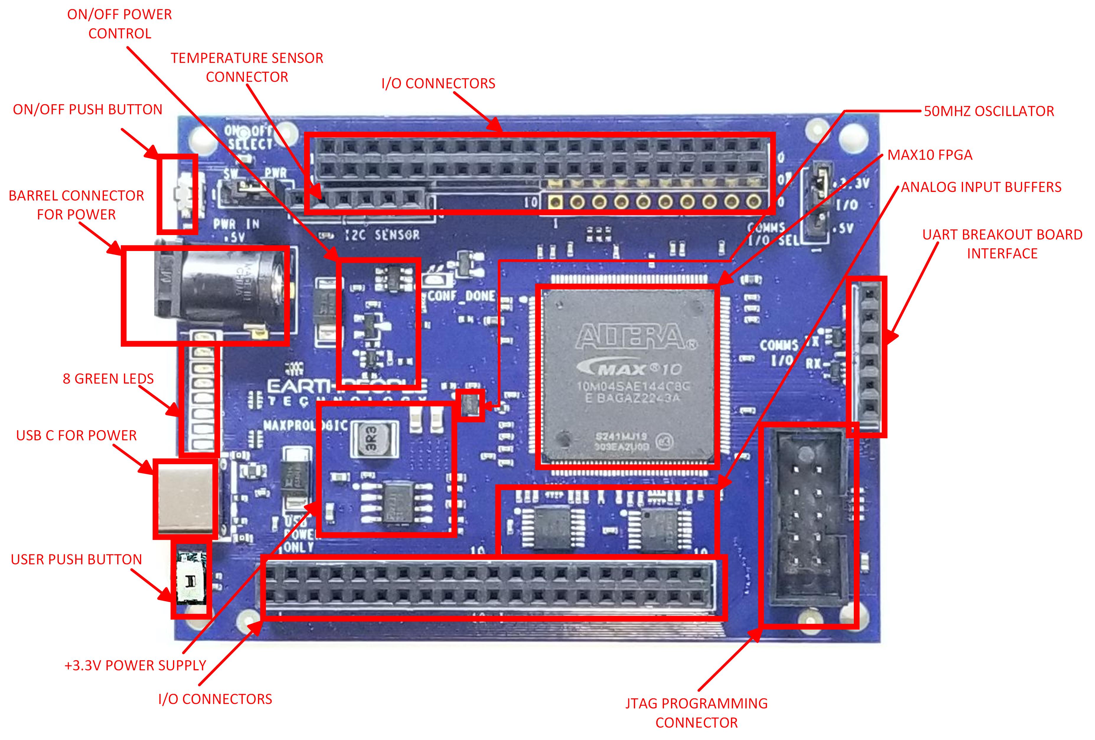
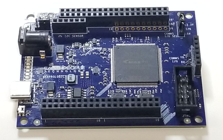
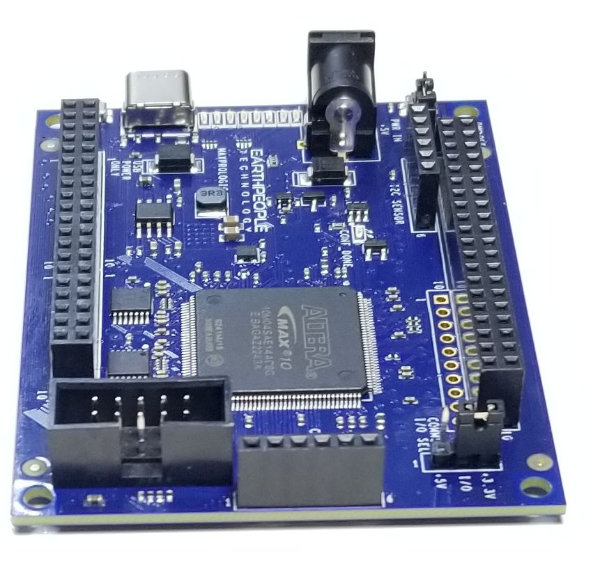
MAXPROLOGIC

|
|
| The MaxProLogic is designed to make digital design easy and cost effective. At Earth People Technology we have years of experience helping students and hobbyists get started with FPGA design. We know that the learning curve in getting started can be a time consuming and frustrating event. So, we created a User Manual that walks the user from unpacking to creating the first project to creating an epic project that will get attention. |
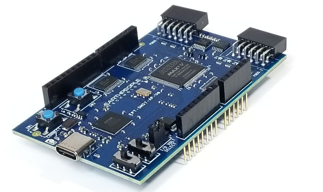
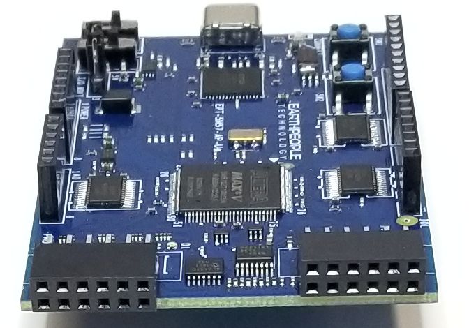
| The core of the MaxProLogic is the Altera MAX10 FPGA. This powerful chip has 4,000 Logic Elements and 200Kbits of Memory. The MAX10 is easily scalable from the entry level college student to the most advanced projects like an audio sound meter with FFT. Upon the many great features of the MaxProLogic is the MAX10 chip has a built |
MaxProLogic FPGA Development System
|
Why the MaxProLogic?
| The MaxProLogic is designed to make digital design easy and cost effective. At Earth People Technology we have years of experience helping students and hobbyists get started with FPGA design. We know that the learning curve in getting started can be a time consuming and frustrating event. So, we created a User Manual that walks the user from unpacking to creating the first project to creating an epic project that will get attention. The Learning Curve with any new piece of hardware is always time consuming. |
|
| In short, the MaxProLogic will cut the time to get the time to get up and running significantly. We also include several pre-made, fully compiled, fully synthesized projects for the user. You can start your project by copying one of these premade projects and adding user code. |
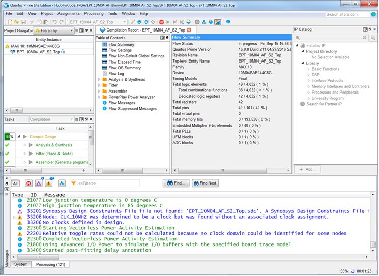
THE MAXPROLOGIC AND SIMULATION
| Simulation has always been a weak point for students and hobbyists. Most FPGA beginners write the user code, compile it, synthesize it, program the chip then test out the results. While this approach may work for small, simple designs, it quickly becomes a problem with larger projects. As the user code increases in complexity, better development tools are required to quickly isolate problems. The premier method for this is functional testing. ModelSim is included Free with the Quartus Prime Package. ModelSim is a powerful tool for finding errors in the user code before you go to synthesis. Earth People Technology has created a guide that walks the user through |
|

PROGRAMMING TOOLS FOR THE MAXPROLOGIC
| The MaxProLogic leverages the Quartus Prime Lite Software for compilation and synethsis. This software tool is completely free and provides very powerful tools for the user. Also included free in the software tools is the simulation tool, ModelSim. A lot beginners to the FPGA world are hesitant about using simulation tools. They feel these tools are too difficult to learn and use. This is where the MaxProLogic breaks that fear. The MaxProLogic comes with a user guide that walks the user from start up to full simulation. Each step is well documented and explained. |
THE MAXPROLOGIC HARDWARE
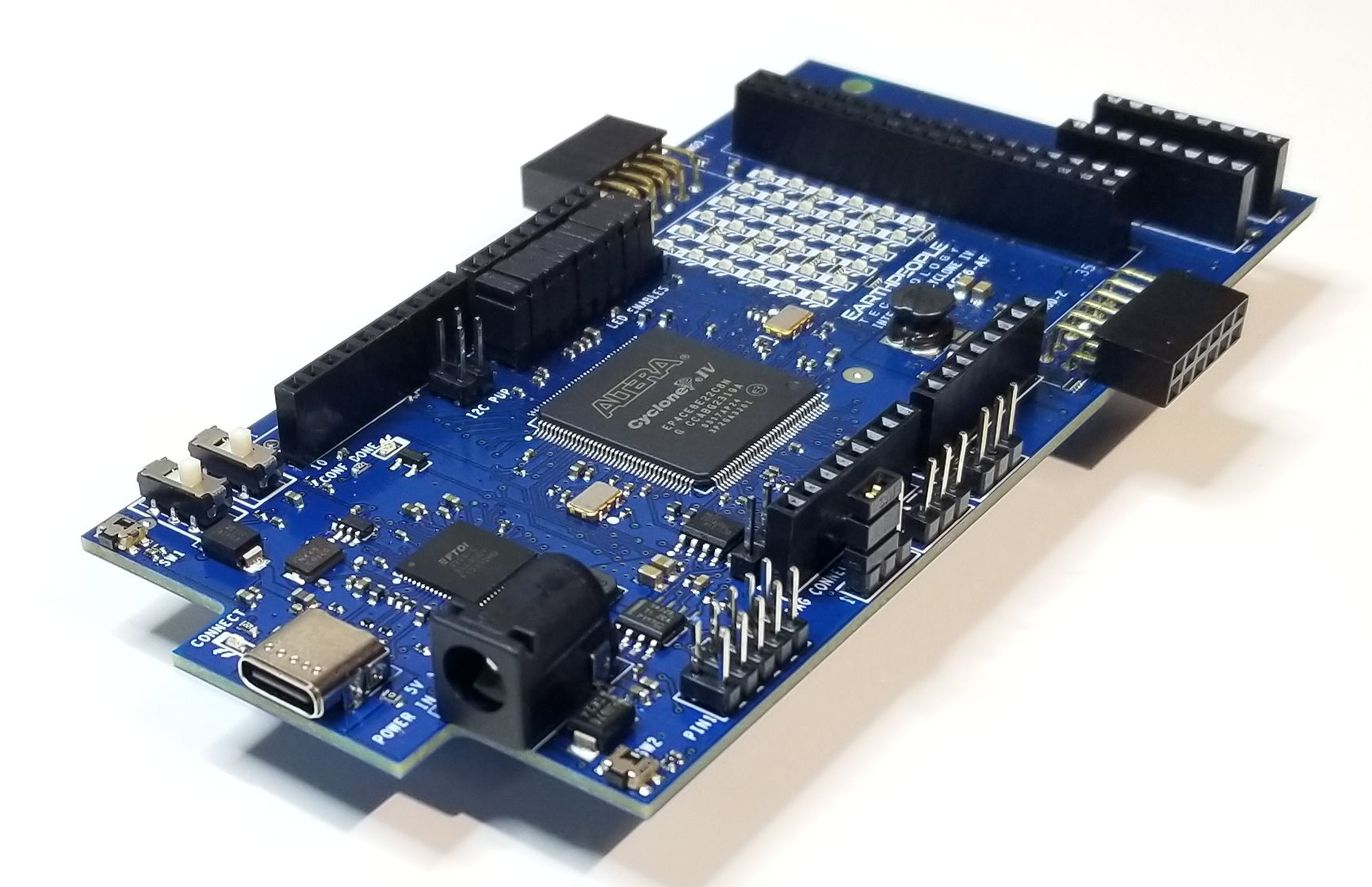
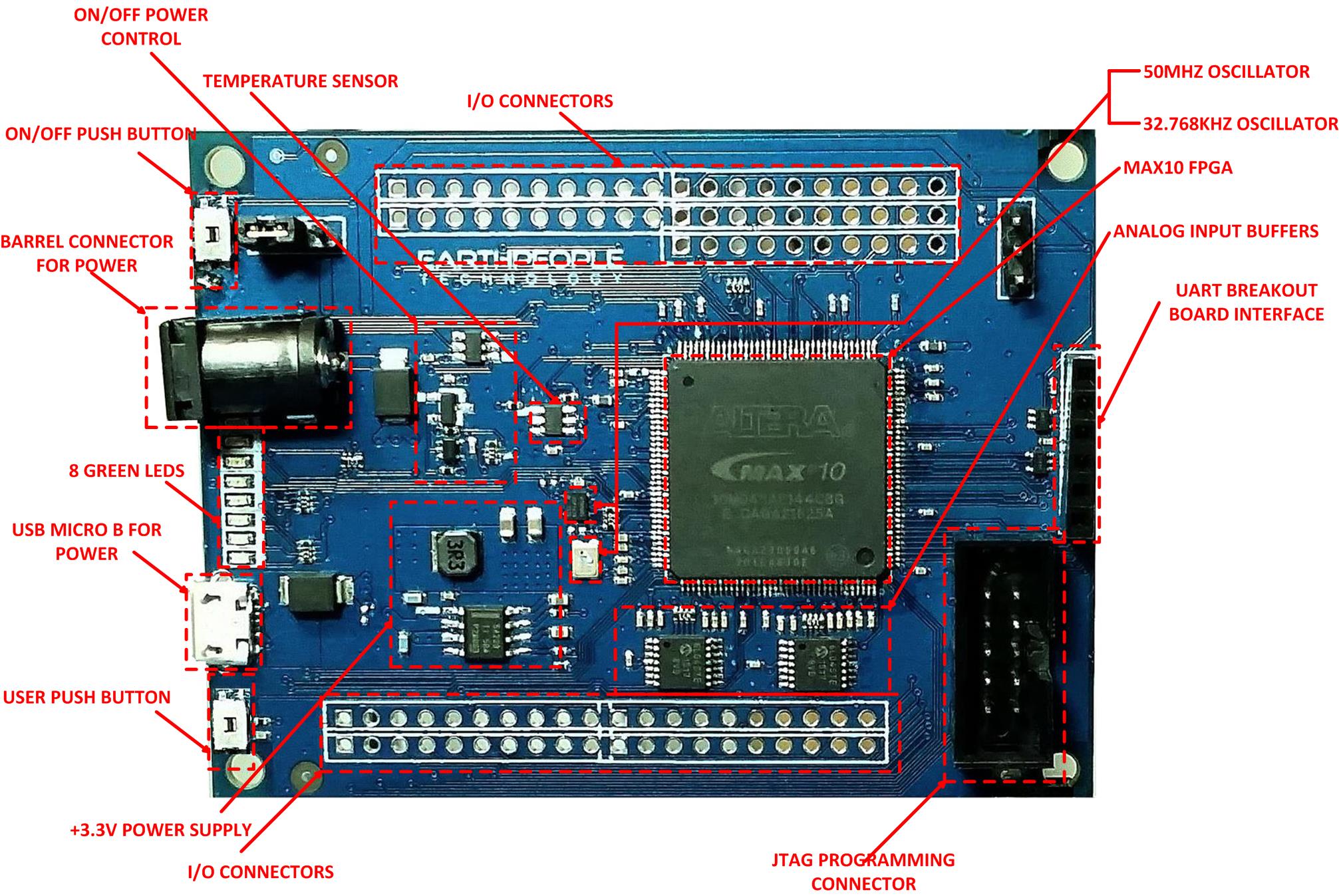
| The MaxProLogic is Open Source Hardware based on the MAX10 FPGA. In addition to the on chip 8 Channel ADC and on chip Flash, the board is loaded with great tools. The board has two power options, standard USB Micro B connector and 5.5mm Barrel connector. You can run the MaxProLogic from a laptop with 2.5W of power. Or you can run it from the +5V @ 2A wall USB chargers for 10W of power. The barrel connector can handle up to +9V @ 3 A for 27W of power. The MaxProLogic has a MicroSD connector on the bottom of the |
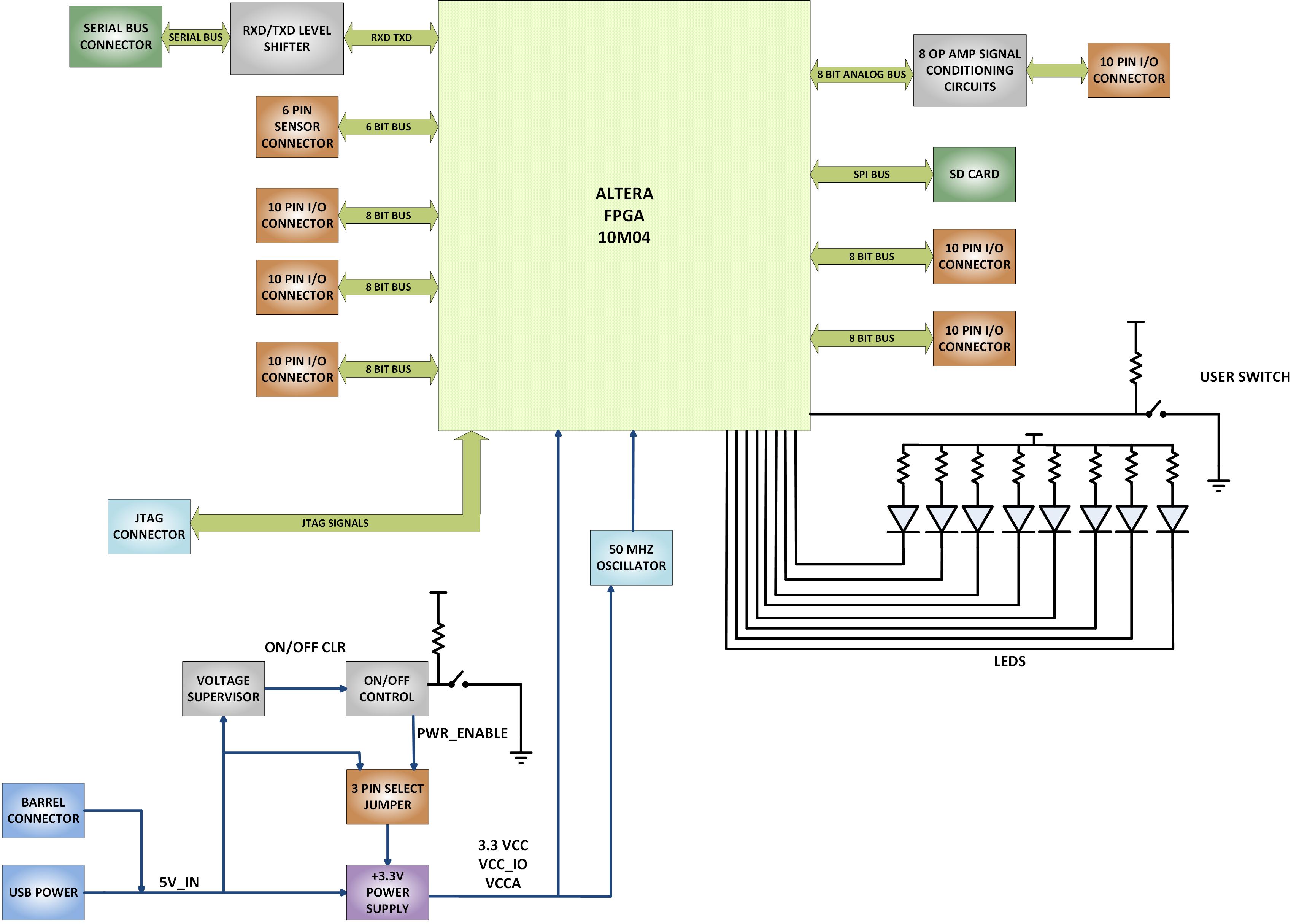
| The block diagram shows all of the parts of the MaxProLogic. There is a main switching power supply for +3.3V. The +3.3V powers the core of the FPGA along with the Input/Outputs of the FPGA as well as provides power for user circuits. |
MaxPrologic Communications
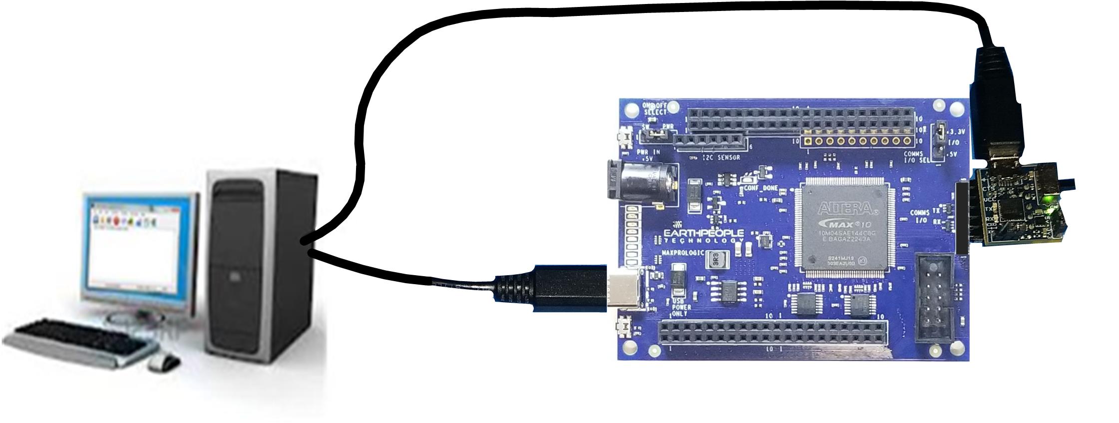
| The MaxProLogic has a built in connector to allow FTDI Breakout Boards or Equivalent to connect directly to the FPGA. There are two voltage level translators that allow both +5V and +3.3V devices to communicate via UART with the FPGA. |
Downloads
| 85-000012 | MaxProLogic FPGA Development System User Manual | MAX_FPGA_DEV_SYS_UM.pdf |
| 95-000013 | MaxProLogic FPGA Development System Data Sheet | MAX_FPGA_DEV_SYS_DS.pdf |
| 45-000013 | MaxProLogic FPGA Development System Project DVD | MAXPROLOGIC FPGA PROJECT DVD |
| 55-000013 | MaxProLogic FPGA Development System Schematics | MaxProLogic SCHEMATICS.pdf |
| 35-000001 | EPT Drivers | CDM212364_SETUP.ZIP |
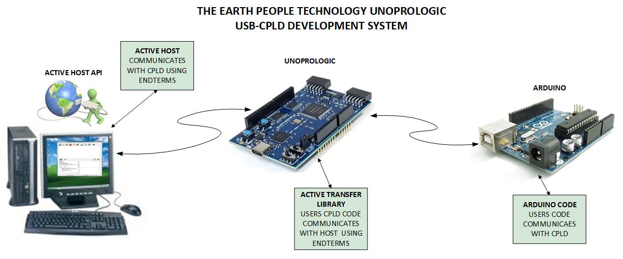
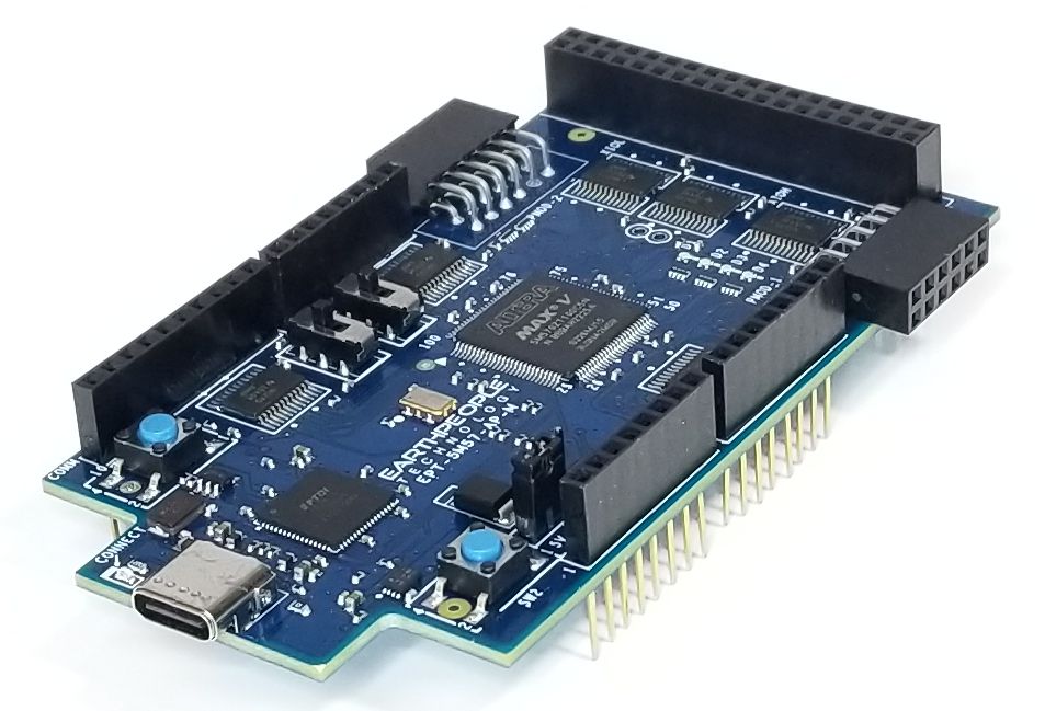
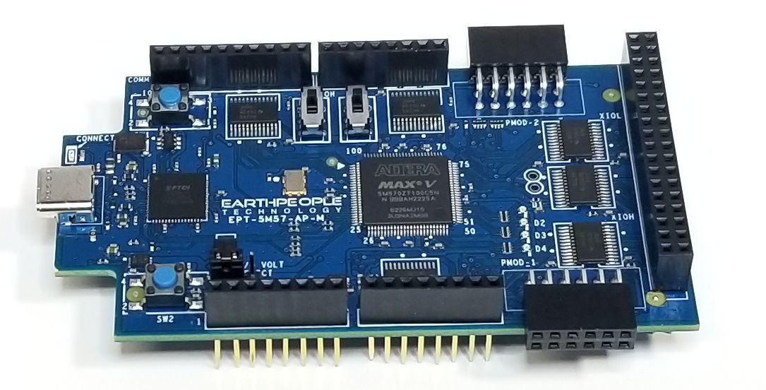
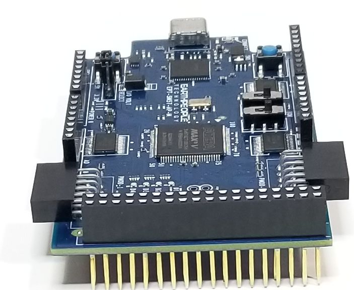
UnoProLogic USB-CPLD Development System

UNOPROLOGIC USB-CPLD
DEVELOPMENT
SYSTEM
The UnoProLogic is an easy to use
CPLD development system. It includes
a four Channel ADC and built in
programmer
| The UnoProLogic makes programmable logic easy with an all inclusive development platform. It includes an Altera 5M570 CPLD, JTAG programmer, and a four channel ADC with 300KS/second sample rate. You can create your HDL code, program it into the CPLD and interact with the hardware via a Windows PC. |

Hardware Features:
|
| The UnoProLogic DVD provides detailed step by step instructions to quickly guide the user to create a project. Once the Quartus software is on your desktop, we will show you how to create a project, write you first LED blinky code, compile and program the CPLD. |
|
Programming the CPLD
| The CPLD on the UnoProLogic can be programmed with the code created by the user. Programming is quick and easy. All that is required is a standard USB-C cable and the Quartus Software installed on the PC. There are no extra parts to buy – just plug in the USB cable and connect the UnoProLogic to the PC |
![]()
![]()
Arduino Compatibility
| The UnoProLogic has four stackable headers that positioned to allow connection with the Arduino Uno. You can use the CPLD to perform high speed communications, multi sensor fusing or extra storage capacity. |
Connecting To Hobby Electronics Made Easy
| The UnoProLogic easily connects to other Hobby Electronics. The durable 74LVC82245 Bus Transceivers allow up to 50mA per Output on the Stackable Headers. This kind of power can drive all kinds of electronics such as long distance cables, LEDs, and high speed electronics. |

Programmable Logic Code Development
| It also provides a high speed data transfer mechanism between an Arduino board and a host PC. The EPT USB-CPLD development system provides a convenient, user-friendly work flow byconnecting seamlessly with Intel’s Quartus Prime Lite software. The user will develop the code in the Quartus environment on a Windows Personal Computer. The programmable logic code is loaded into the CPLD using only the Quartus Programmer tool and a standard USB cable. The Active Host SDK provides a highly configurable communications interface between Arduino and host. It connects tsransparently with the Active Transfer Library in the CPLD code. This Active Host/Active Transfer combination eliminates the complexity of designing a USB communication system. No scheduling USB transfers, USB driver interface or inf file changes are needed. The EPT USB-CPLD development systemis a unique combination of hardware and software. |
| Use the C# examples included in the DVD to create your own display Window on the PC.The user comes complete with tutorial to instruct the user to easily build a Windows program that can display any data from your Arduino or other electronic device. The C# interface uses similar function calls to the Arduino function calls. |
4 Channel Analog to Digital Converter
| Examine four analog channels running up to 300 KSamples/second. The hardware has been simplified to remove extra cost. The input signals are limited to 0 to +5Volts and the sample rate is shared across all four channels. If you run one channel only, it will take advantage of the 300KSamples/second. If you run four channels, each channel will have a maximum sample rate of 75 KSamples/second. |
The UnoProLyzer Application
| The UnoProLyzer is an Open Source Oscilloscope Application created by Earth People Technology. This application runs on a Windows PC. It sends commands to and receives the data from the UnoProLogic and stores each channel data in its own separate buffer in memory. The UnoProLyzer collects all samples from each channel by streaming across up to four dedicated communication “pipes”. The traditional USB oscilloscope performs all of its functions down at the hardware level. This includes |
|
| These scopes will then send the selected data to be displayed on a laptop. Effectively using the laptop as a dumb terminal. However, the modern laptop is extremely powerful with multi-core processors and multi-threaded operating systems. So, why not take advantage of the processing power on the laptop. This is what the UnoProLogic and UnoProLyzer do so well. The UnoProLogic commands the ADC to start a conversion on the channels selected by the user. It then waits for the ADC to complete the conversion on all channels. It transfers the data for each channel across its own dedicated communication pipe. Then starts the process over again. The UnoProLyzer application will accept each data word and decode the pipe number it came across. It stores each word into a separate buffer for each channel. The UnoProLyzer then performs post processing on each data word. It performs trigger detection, smoothing, sorting, scaling and searching. It then displays the data set in 500 data point segments. |
Programming Features:
|
Kit Contents
| UnoProLogic kit contains the UnoProLogic and a DVD which includes the User Manual that walks the user through setting up the drivers, software, how to use to the test application. There is also a full tutorial in writing your first CPLD project, C# application and Arduino code. All the code for the projects are included. |
Downloads
| 85-000010 | UnoProLogic USB/PLD Development System User Manual | UNO_USB_CPLD_DEV_SYS_UM.pdf |
| 95-000010 | UnoProLogic USB/PLD Development System Data Sheet | UNO_USB_CPLD_DEV_SYS_DS.pdf |
| 45-000010 | UnoProLogic USB-CPLD Development System Project DVD | UNO_USB_CPLD_PROJECT_DVD |
| 55-000010 | UnoProLogic USB-CPLD Development System Schematics | UNOPROLOGIC_SCHEMATICS.PDF |
| 35-000001 | EPT Drivers | CDM212364_Setup.ZIP |
MegaProLogic Development Board for Arduino 2560 Mega
The MegaProLogic is an easy to use
CPLD development system.
Purchase at these webstores:
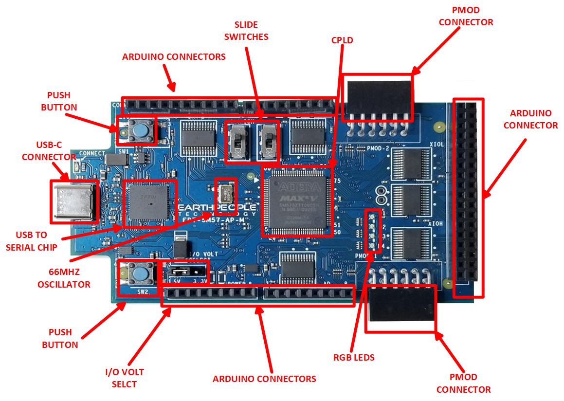
| The MegaProLogic makes programmable logic easy with an all inclusive development platform. It includes an Altera 5M570 CPLD, JTAG programmer, and a 32 General Purpose Inputs/Outputs. You can create your HDL code, program it into the CPLD and interact with the hardware via a Windows PC. |

Hardware Features:
|
| The MegaProLogic DVD provides detailed step by step instructions to quickly guide the user to create a project. The entire Quartus Prime Lite software is included on the DVD. This let’s you bypass the lengthly download process involved in getting the 3.6 GB file. Once the Quartus software is on your desktop, we will show you how to create a project, write you first LED blinky code, compile and program the CPLD. |
|
Programming the CPLD
| The CPLD on the MegaProLogic can be programmed with the code created by the user. Programming is quick and easy. All that is required is a standard USB cable with a Micro B connector and the Quartus Software installed on the PC. There are no extra parts to buy – just plug in the USB cable and connect the MegaProLogic to the PC |
![]()
Connecting To Hobby Electronics Made Easy
| The MegaProLogic easily connects to other Hobby Electronics. The durable 74LVC82245 Bus Transceivers allow up to 50mA per Output on the Stackable Headers. This kind of power can drive all kinds of electronics such as long distance cables, LEDs, and high speed electronics. |
Programmable Logic Code Development
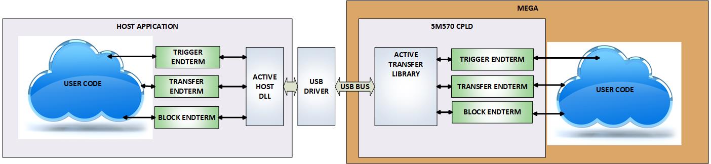
| It also provides a high speed data transfer mechanism between the MegaProLogic board and a host PC. The MegaProLogic development system provides a convenient, user-friendly work flow by connecting seamlessly with Altera’s Quartus Prime Lite software. The user will develop the code in the Quartus environment on a Windows Personal Computer. The programmable logic code is loaded into the CPLD using only the Quartus Programmer tool and a standard USB cable. The Active Host SDK provides a highly configurable communications interface between CPLD and host. It connects transparently with the Active Transfer Library in the CPLD code. This Active Host/Active Transfer combination eliminates the complexity of designing a USB communication system. No scheduling USB transfers, USB driver interface or inf file changes are needed. The MegaProLogic development systemis a unique combination of hardware and software. |
| Use the C# examples included in the DVD to create your own display Window on the PC.The user comes complete with tutorial to instruct the user to easily build a Windows program that can display any data from user code or other electronic device. The C# interface uses similar function calls to the Arduino function calls. |
Programming Features:
|
Kit Contents
| MegaProLogic kit contains the MegaProLogic and a DVD which includes the User Manual that walks the user through setting up the drivers, software, and the test application. There is also a full tutorial in writing your first CPLD project and C# application. All the code for the projects are included. |
Downloads
| 85-000040 | MegaProLogic CPLD Development System User Manual | MEGA_USB_CPLD_DEV_SYS_UM.pdf |
| 95-000040 | MegaProLogic CPLD Development System Data Sheet | MEGA_USB_CPLD_DEV_SYS_DS.pdf |
| 45-000040 | MegaProLogic CPLD Development System Project DVD | MEGAPROLOGIC_USB_CPLD_PROJECT_4.5_DVD |
| 55-000040 | MegaProLogic CPLD Development System Schematics | MEGAPROLOGIC_SCHEMATICS.PDF |
| 35-000001 | EPT Drivers | EPT_2.08.24.ZIP |
EPT-220X-DB-U2 SPI Slave Communications Board for Arduino Uno
 EPT-220X-DB-U2
The EPT 220X-DB-U2 is designed to support the Uno board of the Arduino Open source Prototyping Platform. The Uno can communicate as an SPI Master to an SPI Slave device. The EPT 220X-DB-U2 is a USB to Slave SPI device. This will allows users to communicate from the Arduino Uno board to the PC over SPI. Use the Active Host API to quickly and easily create a simulated SPI sensor on the PC. Use the simulated SPI Sensor to debug your Arduino SPI Master commnication code.
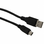 The EPT-220X-DB-U2 Requires the use of a USB Mini Type B cable. EPT recommends the EPT-USB-AM-MB cable.
Features:
- Uses FTDI 220X IC Chip
- USB to Slave SPI Interface
- Data transfer rates to 500 Kbytes/sec
- +5V I/O compatible
- Supported by Active Host API
Downloads
| 85-000003 | UNO SPI Slave to USB User Manual | UNO_SPI_USB_UM.pdf |
| 95-000003 | UNO SPI Slave to USB Data Sheet | UNO_SPI_USB_DS.pdf |
| 45-000003 | UNO SPI Slave Project CD | UNO_SPI_PROJECT_CD.ZIP |
| 35-000001 | EPT Drivers | EPT_2.08.24.ZIP |
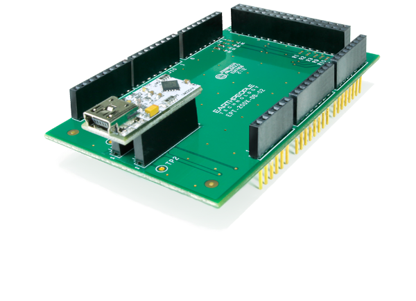
EPT-201X-DB-M4 I2C Slave Communications Board for the Arduino 2560 Mega
 EPT-201X-DB-M4 and I2C Slave Communications Board
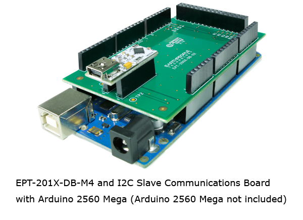
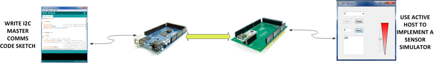
The EPT-201X-DB-M4 is designed to support the Uno board of the Arduino Open source Prototyping Platform. The Mega can communicate as an I2C Master to an I2C Slave device. The EPT-201X-DB-M4 is a USB to Slave I2C device. This will allows users to communicate from the Arduino Mega board to the PC over I2C. Use the Active Host API to quickly and easily create a simulated I2C sensor on the PC. Use the simulated I2C Sensor to debug your Arduino I2C Master communication code.
The EPT-201X-DB-M4 I2C Slave Communications Board can communicate directly with Hyper Serial Port to provide a serial terminal for debugging the Arduino I2C Master communications. You can easily create your own I2C communications and debug it using the EPT-201X-DB-M4.
The EPT-201X-DB-M4 Requires the use of a USB Mini Type B cable. EPT recommends the EPT-USB-AM-MB cable.Features:
- Uses FTDI 201X IC Chip
- USB to Slave I2C Interface
- Up to 3.4 MHz, high speed mode, I2C supported
- +5V I/O compatible
- Supported by Active Host API
Downloads
| 85-000006 | MEGA I2C Slave to USB User Manual | MEGA_I2C_USB_UM.pdf |
| 95-000006 | MEGA I2C Slave to USB Data Sheet | MEGA_I2C_USB_DS.pdf |
| 45-000006 | MEGA I2C Slave Project CD | MEGA_I2C_PROJECT_CD.ZIP |
| 35-000001 | EPT Drivers | EPT_2.08.24.ZIP |
EPT 201X-DB-U2 I2C Slave Communications Board for the Arduino Uno
 EPT 201X-DB-U2 I2C Slave Communications Board
The EPT 201X-DB-U2 is designed to support the Uno board of the Arduino Open source Prototyping Platform. The Uno can communicate as an I2C Master to an I2C Slave device. The EPT 201X-DB-U2 is a USB to Slave I2C device. This will allows users to communicate from the Arduino Uno board to the PC over I2C. Use the Active Host API to quickly and easily create a simulated I2C sensor on the PC. Use the simulated I2C Sensor to debug your Arduino I2C Master communication code.
The EPT 201X-DB-U2 I2C Slave Communications Board can communicate directly with HyperSerialPortTM to provide a serial terminal for debugging the Arduino I2C Master communications. You can easily create your own I2C communications and debug it using the EPT 201X-DB-U2.
The EPT-201X-DB-U2 Requires the use of a USB Mini Type B cable. EPT recommends the EPT-USB-AM-MB cable.Features:
- Uses FTDI 201X IC Chip
- USB to Slave I2C Interface
- Up to 3.4 MHz, high speed mode, I2C supported
- +5V I/O compatible
- Supported by Active Host API
Downloads
| 85-000005 | UNO I2C Slave to USB User Manual | UNO_I2C_USB_UM.pdf |
| 95-000005 | UNO I2C Slave to USB Data Sheet | UNO_I2C_USB_DS.pdf |
| 45-000005 | UNO I2C Slave Project CD | UNO_I2C_PROJECT_CD.ZIP |
| 35-000001 | EPT Drivers | EPT_2.08.24.ZIP |
EPT-220X-DB-M4 SPI Slave Communications Board for Arduino 2560 Mega
 EPT-220X-DB-M4 and SPI Slave Communications Board
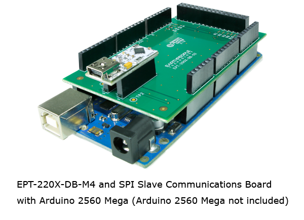
The EPT-220X-DB-M4 is designed to support the Uno board of the Arduino Open source Prototyping Platform. The Mega can communicate as an SPI Master to an SPI Slave device. The EPT-220X-DB-M4 is a USB to Slave SPI device. This will allows users to communicate from the Arduino Mega board to the PC over SPI. Use the Active Host API to quickly and easily create a simulated SPI sensor on the PC. Use the simulated SPI Sensor to debug your Arduino SPI Master communication code.
The EPT-220X-DB-M4 SPI Slave Communications Board can communicate directly with Hyper Serial Port to provide a serial terminal for debugging the Arduino SPI Master communications. You can easily create your own SPI communications and debug it using the EPT-220X-DB-M4.
The EPT-220X-DB-M4 Requires the use of a USB Mini Type B cable. EPT recommends the EPT-USB-AM-MB cable.Features:
- Uses FTDI 220X IC Chip
- USB to Slave SPI Interface
- Data transfer rates to 500 Kbytes/sec
- +5V I/O compatible
- Supported by Active Host API
Downloads
| 85-000005 | MEGA SPI Slave to USB User Manual | MEGA_SPI_USB_UM.pdf |
| 95-000005 | MEGA SPI Slave to USB Data Sheet | MEGA_SPI_USB_DS.pdf |
| 45-000004 | MEGA SPI Slave Project CD | MEGA_SPI_PROJECT_CD.ZIP |
| 35-000001 | EPT Drivers | EPT_2.08.24.ZIP |
EPT 232R-US-R1 USB to Serial 1 meter cable
 The TRX-1226 USB to Serial cable
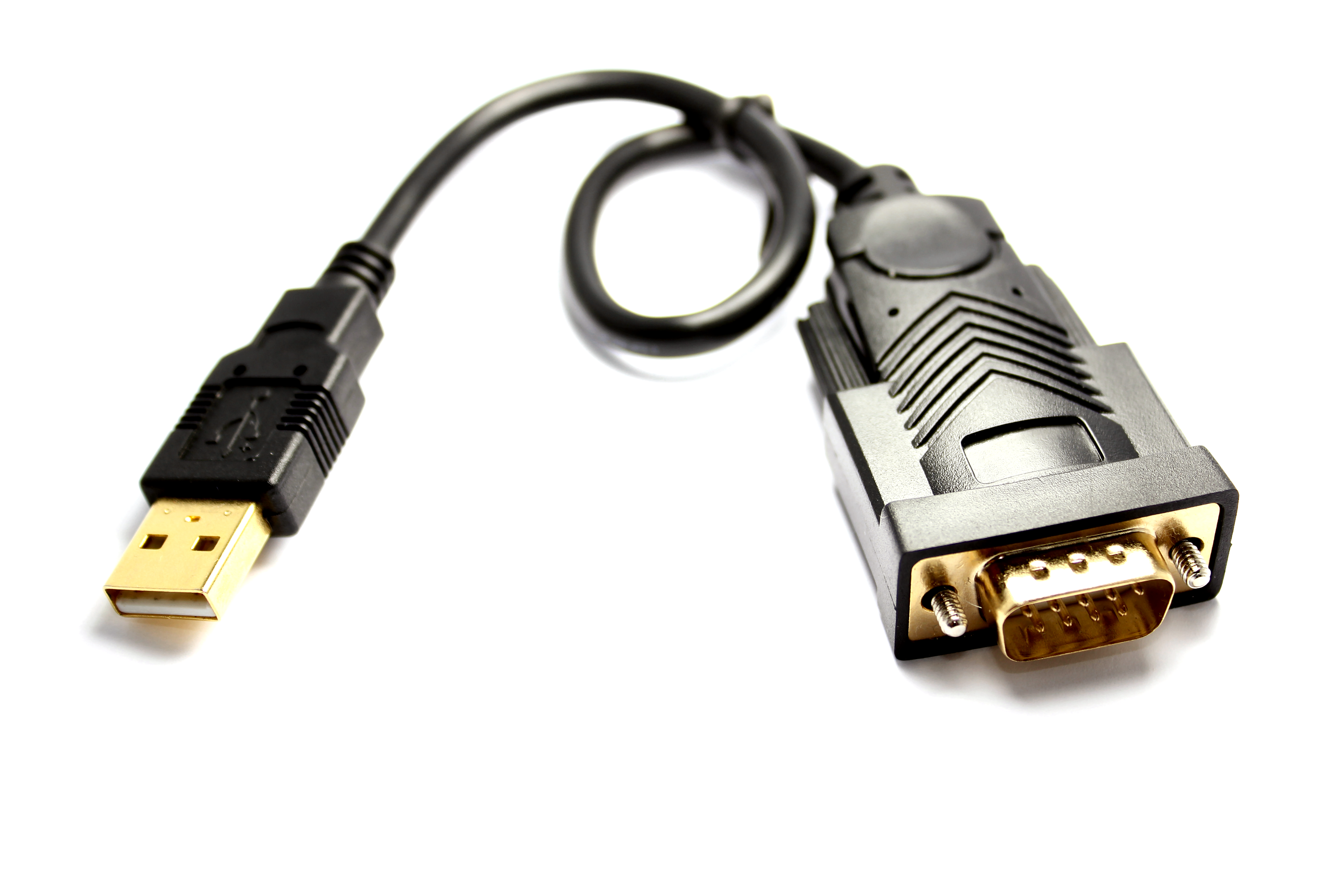 Virtual COM Port
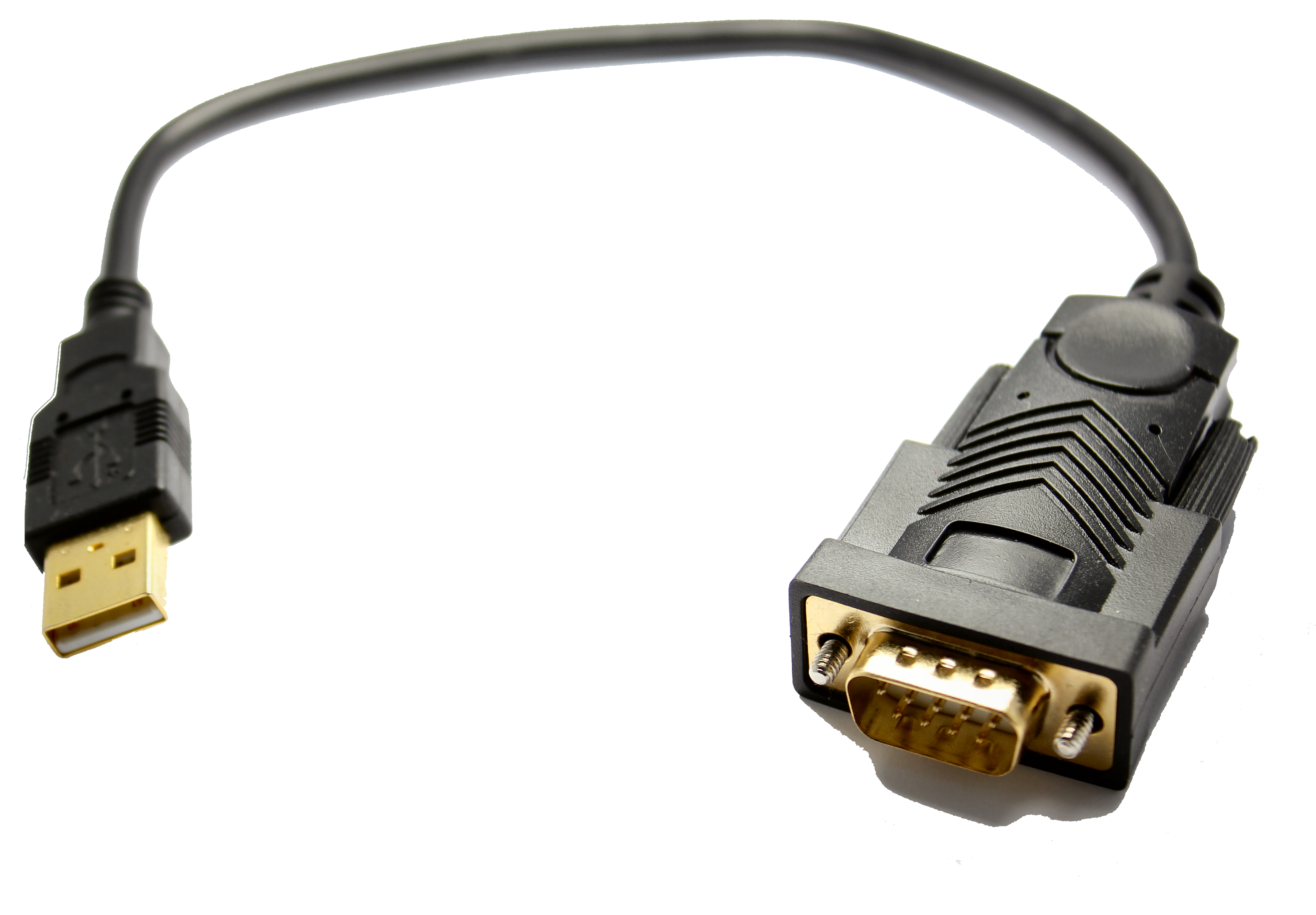 Premium Quality, Gold PLated Connectors, Tough Rubber Exterior
The TRX-1226 USB to Serial cable is a complete solution in adapting legacy serial devices with RS232 interfaces to modern USB ports. Each TRX-1226 adapter contains a small internal electronic circuit board which utilises the FTDI FT232R chip, mounted inside a rugged plastic enclosure capable of withstanding industrial temperature ranges.
The Cable incorporates a standard USB-A device connector for connection to an upstream host or hub port. RS232-level signals, including modem handshake signals, are available on an industry-standard DB-9 Male connector. The maximum RS232-level data rate is 0.5 MBaud. The TRX-1226 adapter cable requires USB device drivers, available from www.earthpeopletechnology.com/resources/drivers, which are used to make the EPT 232R-US-R2 appear as a Virtual COM Port (VCP). This allows existing serial communications software, such as HyperSerialPort, to exchange data through the TRX-1226 to a legacy RS232 peripheral device.
Features:
- Adds one RS-232 serial port by connecting to USB
- Fully supported by HyperSerialPort TM
- Side-lit blue RXD and TXD traffic indicators
- Enhanced RS232 transceiver gives serial port speed of up to 0.5 MBaud
- Easy Plug and Play VCP drivers
- Fully compliant with USB 2.0
- On Board FIFO’s: 128 byte transmit buffer, 256 byte receive buffer
Downloads
| 85-000007 | UNO USB/PLD Development System User Manual | USB to Serial User Manual |
| 95-000007 | UNO USB/PLD Development System DataSheet | USB to Serial Data Sheet |
| 35-000001 | EPT Drivers | CDM20824_SETUP.EXE |
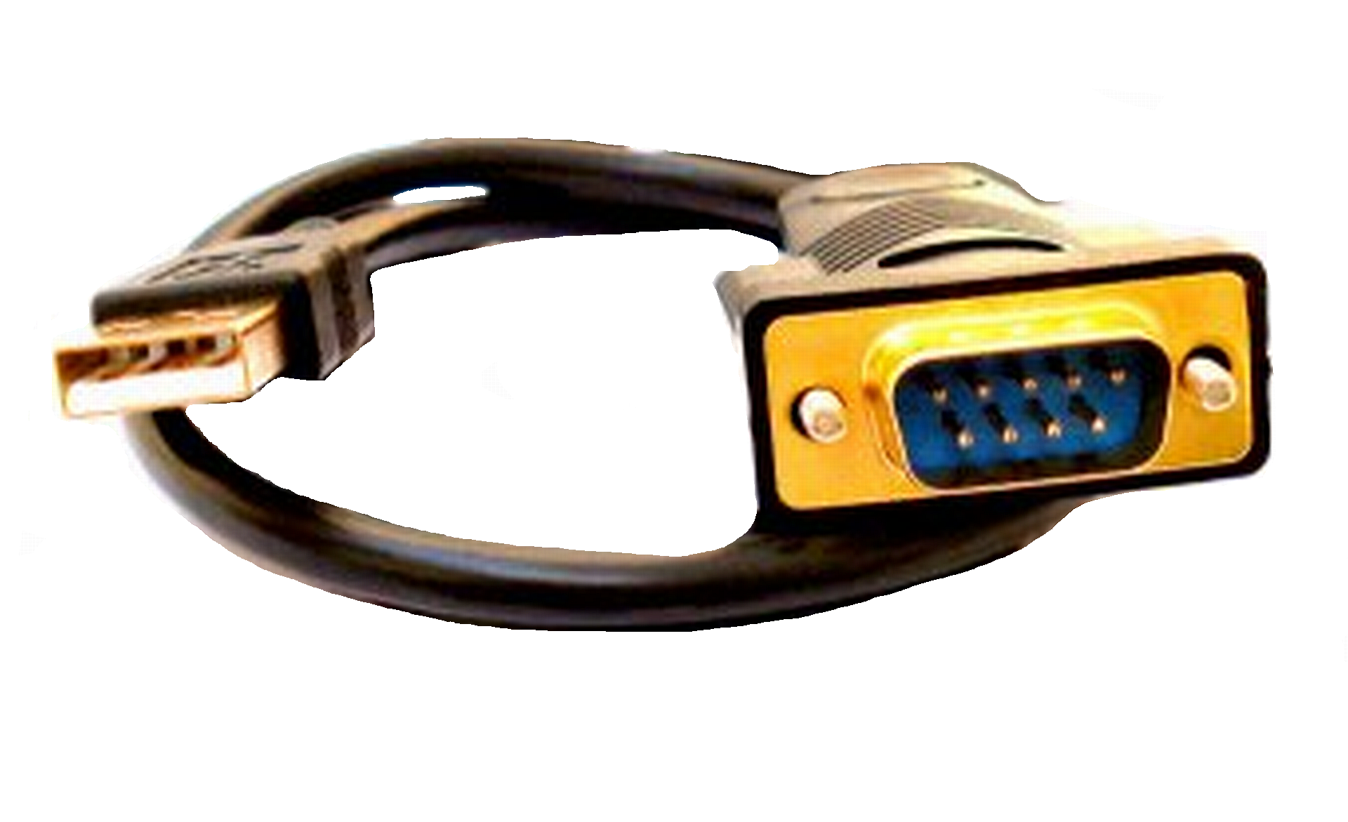
EPT USB-AM-MB USB Mini Type B cable
 EPT USB-AM-MB USB Mini Type B cable
The EPT-USB-AM-MB USB cable provides connection between the USB port on a PC and the EPT USB boards. It is USB 2.0 compliant and capable of transferring data at 480 Mbits/sec. The cable is three feet in length and includes a Type Male connector for the PC and a Mini Type B connector for the Device.
Features:
- Fully compliant with USB 2.0
- A Male to Mini B Male
- 3.00 feet in length
- Shielded cable
- ROHS compliant
Downloads
| 95-000008 | USB Mini B Cable Data Sheet | USB_MINI_B_DS.pdf |
VisiPort2 FTDI Breakout Board
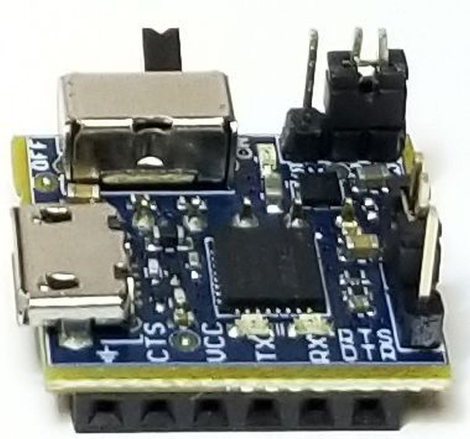 |
VisiPort FTDI Based USB to Serial AdapterThe VisiPort is a USB To Serial Breakout Board. Based on the FT232R Chip, it’s designed to program Arduinos as well as . Its small size allows it to fit into bread board applications where other programmers are too big and bulky. |
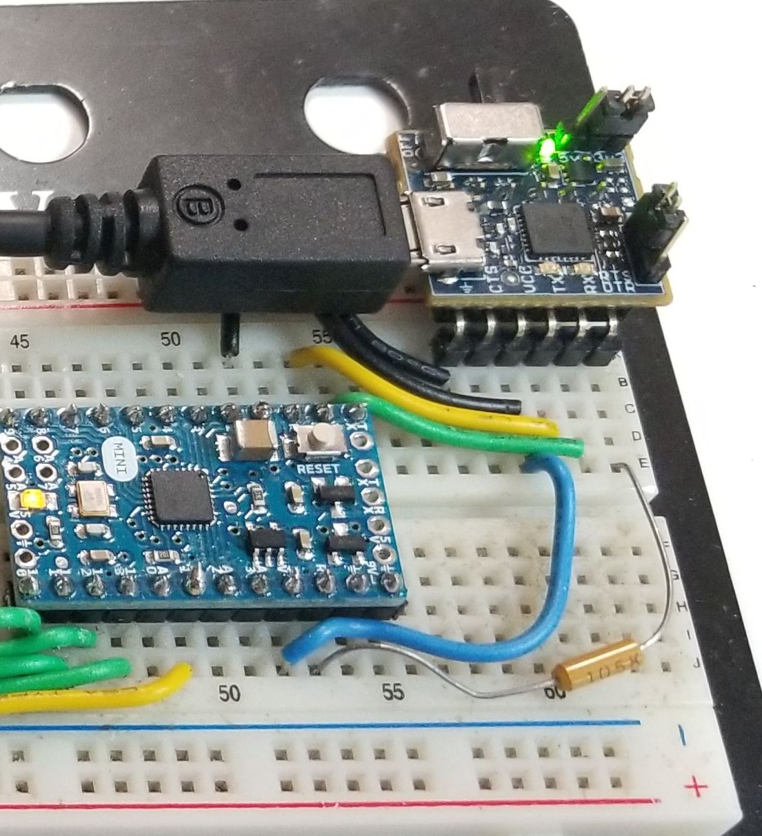
It is designed to program Arduinos.
Its six pin female header connects easily to a Mini Pro with no bread board needed. It has one green LED that indicates power is applied to the FTDI chip. There are two amber LEDs to indicate when Tx and Rx are active.
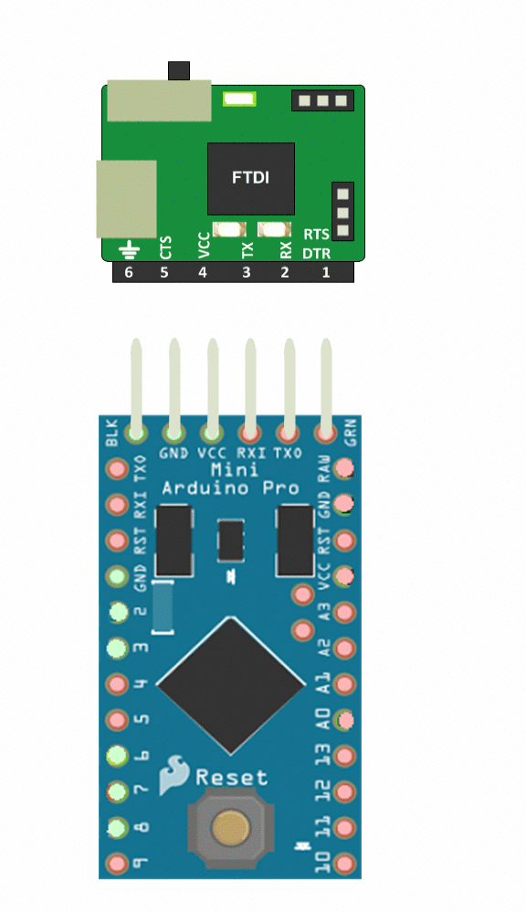
The VisiPort works with 5Volt and 3.3Volt Arduinos
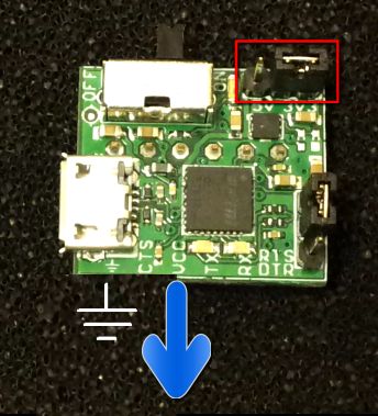
Use the three pin jumper in the upper right corner to select I/O voltage of the VisiPort. This selection allows compatibility with all Arduinos.
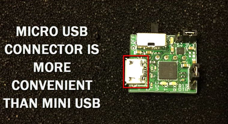
The VisiPort Uses a Micro USB Connector
The Micro USB connector is lower profile and allows cables to connect into the center of the VisiPort. This keeps the overall size smaller than any other programmer.
What’s the difference between VisiPort and other programmers?
- We made the VisiPort as compact as physically possible
- We used a Micro USB connector instead of the Mini USB
- The VisiPort is compatible with 5V or 3.3V Arduinos
- The VisiPort can power your board up to 280 mAs at 3.3V or 480 mAs at 5V
- We gave the VisiPort jumper selectable DTR or RTS reset capability
- We also gave the VisiPort a USB disconnect switch which allows you to turn off the serial port path to the PC and communicate over the serial port to any device with removing the USB cable.
The VisiPort is the perfect tool for debugging microcontrollers. Use it to download your compiled hex file to the flash (using the bootloader of the microcontroller). Use it to communicate with your code and provide debug information about the execution process.
Hardware Features:
- FTDI FT232R USB To Serial Chip
- User Selectable +3.3V and +5V Inputs/Outputs
- Provides up to 450 mA of power for your Arduino
- User Selectable RTS/DTR for programming Arduinos
Programming Features:
- 100% Compatible with all versions of the Arduino Software
- 100% Compatible with all Serial Monitors
- Uses the latest FTDI Driver, Ver 2.12
Downloads
| 85-000009 | VisiPort2 User Manual | VISIPORT2_UM.pdf |
| 95-000009 | VisiPort2 DataSheet | VISIPORT2_DS.pdf |
| 45-000009 | VisiPort2 Project CD | VISIPORT_PROJECT_CD.ZIP |
| 55-000009 | VisiPort2 Schematics | VISIPORT2_SCHEMATICS.PDF |
| 35-000001 | CDM Drivers | CDM_2.12.00.EXE |
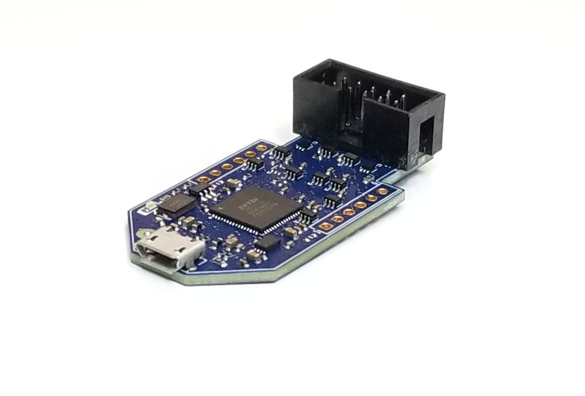
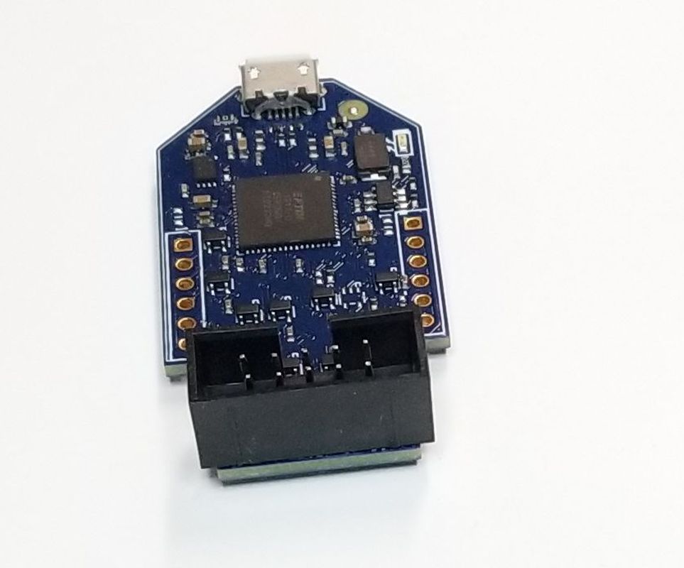
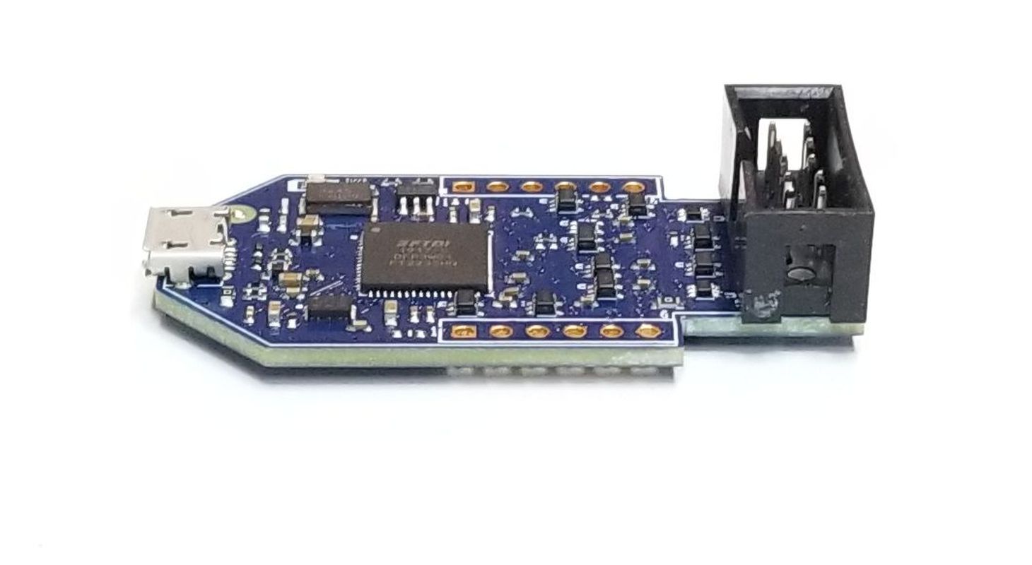
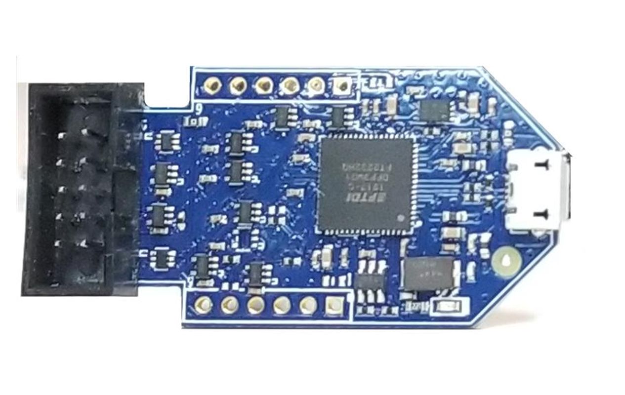
FTDI DUAL CHANNEL BREAKOUT BOARD
Dual Channel FTDI Breakout Board
The FTDI
DUAL CHANNEL BREAKOUT BOARD
|
This breakout board is based on the FTDI FT2232H USB 2.0 IO chip. The FT2232H |
|
The FT2232H Breakout Board contains the MPSEE engine. This engine can output SPI, I2C, JTAG or act like an eight bit parallel port. Using the JTAG interface, the FTDI Breakout Board can program the ATMega and Arduinos. It is supported by OpenOCD, urJTAG and others. Hardware Features: |
|
|
|
|
The breakout board includes an external EEPROM for custom USB descriptors and VID/PIDs, Serial Numbers, Driver selection (Virtual COM Port or D2XX drivers). There are two 13×2 Headers on 0.1 inch pitch installed on the bottom of the board. An external +3.3V LDO provides power for the FT2232H chip as well as powering off board electronics. The FT2232H chip can operate up to 12MBaud data transfer rates via USB 2.0. It features the USB Micro-B connector. |
Downloads
| 85-000001 | Dual Channel FTDI Breakout Board User Manual | DUAL_CH_FTDI_BREAKOUT_UM.pdf |
| 95-000001 | Dual Channel FTDI Breakout Board DataSheet | DUAL_CH_FTDI_BREAKOUT_DS.pdf |
| 55-000001 | Dual Channel FTDI Breakout Board Schematics | DUAL_CH_FTDI_BREAKOUT_SCHEMATIC.PDF |
| 35-000001 | EPT Drivers | EPT_2.12.00.exe |
USB Micro B Cable
EPT-218-UC-R2 USB Micro Type B cable
USB 2.0 A Male to Micro-B Male 28/24 AWG High-Speed Shielded Data & Charging Cable
High Performance USB 2.0 Micro B Cable
| The EPT-218-UC-R2 USB cable provides connection between the USB port on a PC and the EPT USB boards. It is USB 2.0 compliant and capable of transferring data at 480 Mbits/sec. The cable is three feet in length and includes a Type Male connector for the PC and a Micro Type B connector for the Device. |
.jpg)
.jpg)
.jpg)
.jpg)
- Top/premium quality, flexible & durable.
- Outstanding micro-USB retention, snug fit/no wiggle (unlike others on eBay that have been compared).
- Molded connector hood for strain relief.
- This standard uUSB micro-USB works with many cell phones and small electronic devices – Droid, HTC and many others.
- 2A+ charging.
- 5 pin
- Black
- Cable 122cm AWM 2725 braid & foil shield, drain wire, 28AWG/1P 24AWG/2C, 4.6m diameter
- RoHS & Lead-Free
- Twist tied in PE bag
- ~45g (1.6oz)
Price: $3.65 Shipping:$0.00 Updating cart…
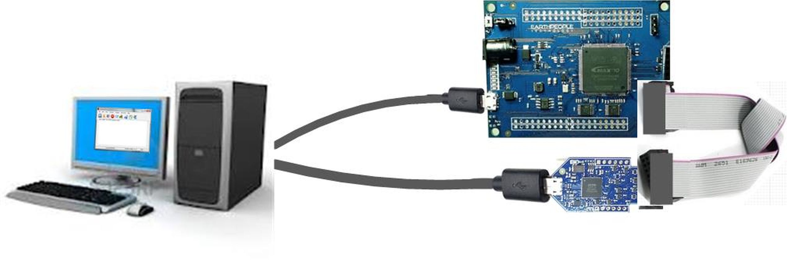
Odin-Link BLE Plus MaxProLogic Development Kit
|
|
 |
 Odin-Link BLE Plus MaxProLogic Development Kit
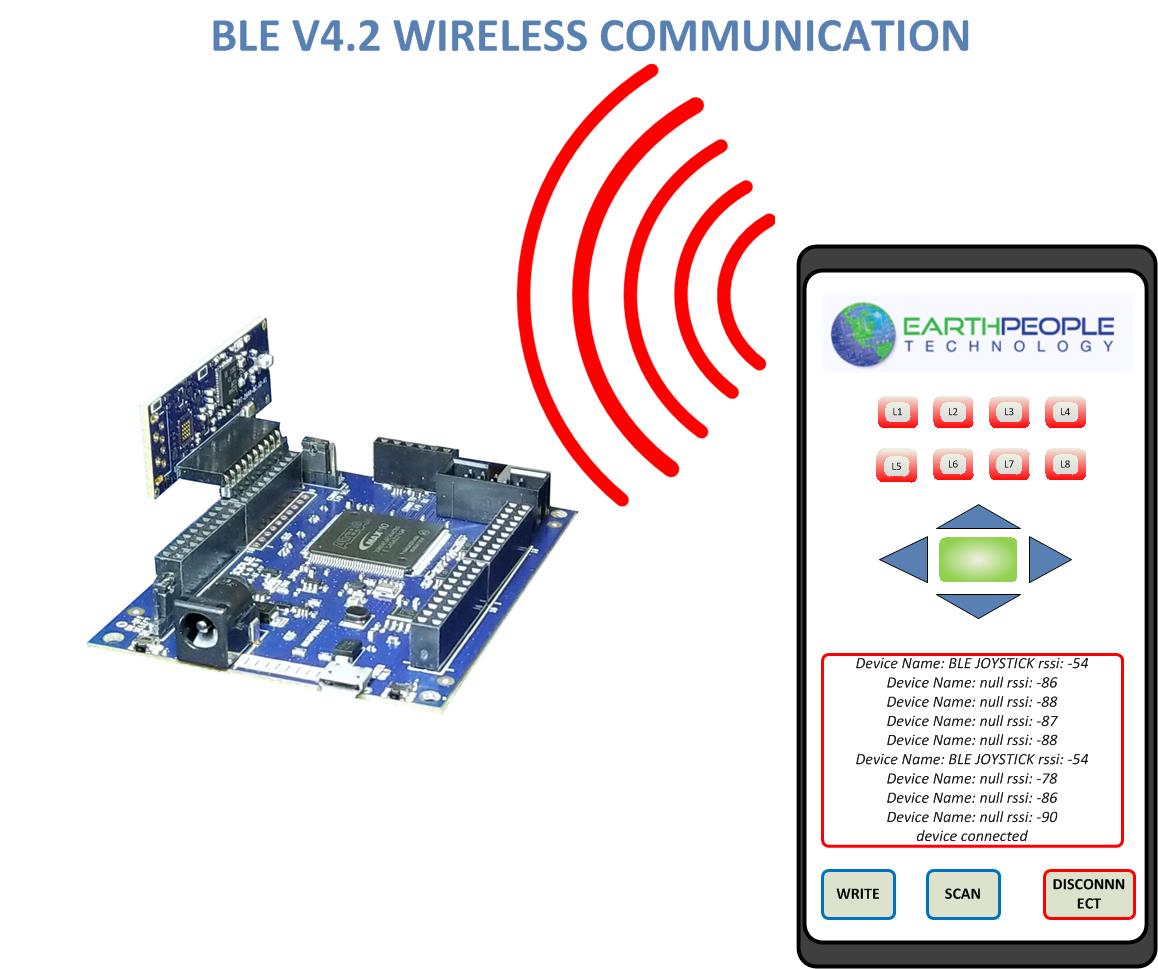
The Odin-Link BLE Plus MaxProLogic Development System
Provides the Easiest Way to Add BLE to any DIY Project.
| The Odin-Link plus MaxProLogic is the simplest BLE development kit on the market. The Android phone app, included with the kit, is completely self contained, there is no programming or third party provider access. Just load the “JoyStick.apk” onto your Android phone and start sending commands to the Odin-Link. Most BLE development kits require a third party provider to build a custom Phone app. Because of this, the user must build the phone app, compile the phone app, then load it onto an Android Phone. |
Kit Contents
| The kit is ready to use out of the box. You will need a USB Micro B cable. |
|
 |
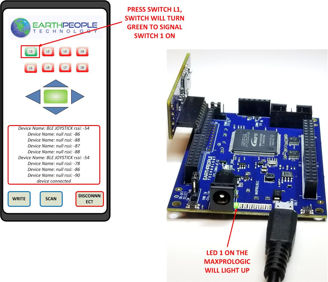
| The JoyStick app is only available for the Android phone. It provides a simple interface to send commands to the Odin-Link board. There are switches to turn lights on and off, buttons to send single commands and a text communication path. Users can build a wide array of DIY projects including remote lamp controller, BLE controlled robot and remote weather station. |
 |
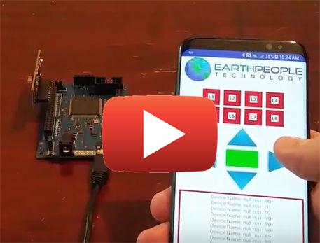 Click For Video Click For Video |
Odin-Link BLE Board
| The Odin-Link BLE board comes pre-programmed with all the profiles required for the JoyStick app to run on an Android phone. No programming is needed for the board. The use of a third party phone app provider to produce a custom app requires programming of the BLE profiles into the BLE chip. This forces the users into writing code, debugging code and programming the BLE chip. The Odin-Link BLE Board development kit eliminates this extra work. It’s virtually plug and play. |
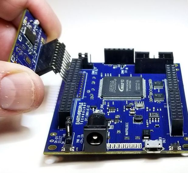 |
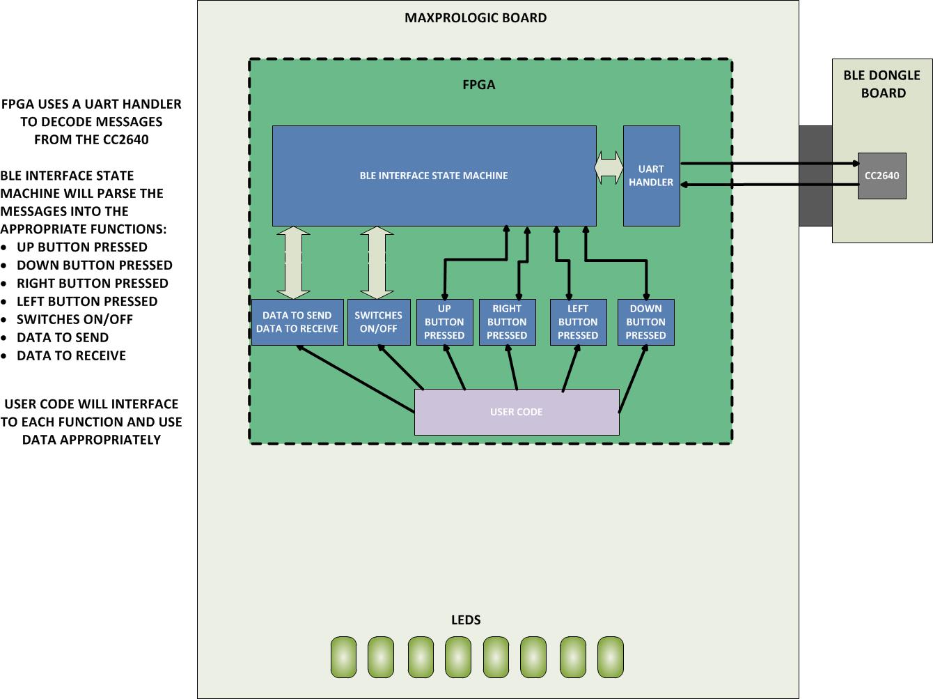
| The Odin-Link BLE board includes a v4.2 BLE chip along with a 2.4GHz antenna and matching network. Texas Instruments provides the CC2640 BLE chip. EPT provided the antenna tuning for maximum RF range. The Odin-Link BLE board plugs directly into the J5 connector of the MaxProLogic. All power and communication happen through through this connector. It communicates with the FPGA over a UART serial link. EPT has created a proprietary Verilog interface that runs in the FPGA and allows full bidirectional communication with the Android phone, via the CC2640 v4.2 chip. |
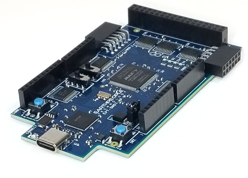
MaxProLogic FPGA Board
|
The MaxProLogic is an FPGA board with the Intel/Altera MAX10 at its heart. The MaxProLogic is an integral piece of the Odin-Link BLE Plus MaxProLogic development kit. It is a standalone FPGA board that is powered by an external source. The onboard switching power supply provides a stable power source for the Odin-Link BLE board. It has a 50MHz ultra low jitter oscillator to provide an array of different clock sources in the FPGA. The Odin-Link BLE plugs directly into the J5 socket of the MaxProLogic. The serial UART signals are connected directly from the CC2640 to the pins on the MAX10 FPGA. |
 |
| The JoyStick Android App takes inputs from the user and generates BLE packets. These BLE packets are transmitted from the Android phone and received by the Odin-Link BLE board. The Odin-Link BLE board decodes the packets and produces ASCII generated commands that are transmitted over the serial UART signals to the MAX10 FPGA. |
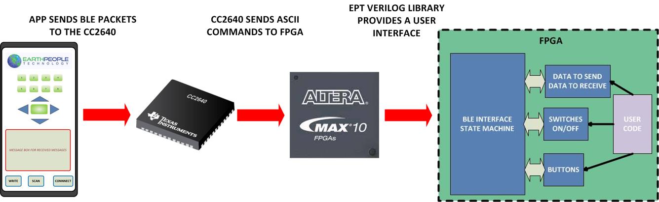 |
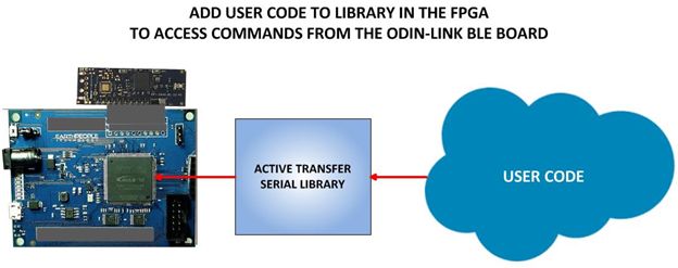
| EPT has created a Verilog library that runs in the MAX10 FPGA to convert the serial ASCII commands into usable signals. The user will interface their code to the library using an easy SDK from EPT. This makes creating advanced projects quick and easy. Just include the library when synthesizing the FPGA project. |
 |
| The Verilog library will parse out each command and send it to the appropriate block interface. There are three block interfaces, buttons, switches and text. There is a demo BLE LED Blinky project included in the DVD. This project allows the user to individually turn on and off the LEDs of the MaxProLogic board. The demo will also allow the user to blink the LEDs in a Blinky Show. The demo project has all the source code, fully compiled project, programming files, and full simulation. |
 |
Downloads
| 105-000001 | Odin-Link + MaxProLogic Development User Manual | ODINLINK_MAXPRO_DEV_SYS_UM.pdf |
| 115-000001 | Odin-Link + MaxProLogic DataSheet | ODINLINK_MAXPRO_DS.pdf |
| 125-000001 | Odin-Link + MaxProLogic Schematics | MAXPROLOGIC_SCHEMATIC.PDF |
| 135-000001 | Odin-Link + MaxProLogic Project DVD | ODINLINK_MAXPRO_DEV_SYS_PROJECT_2.7_DVD.zip |
| 35-000001 | EPT Drivers | EPT_2.12.00.exe |
MegaMax CPLD Development System
The MegaMax is an easy to use
CPLD development system.
Purchase at these webstores:
| The MegaMax makes programmable logic easy with an all inclusive development platform. It includes an Intel 5M570 CPLD, JTAG programmer, and a 32 General Purpose Inputs/Outputs. You can create your HDL code, program it into the CPLD and interact with the hardware via a Windows PC. |
Hardware Features:
|
| The MegaMax DVD provides detailed step by step instructions to quickly guide the user to create a project. The user must download Quartus Prime from the Intel website. Once the Quartus software is on your desktop, we will show you how to create a project, write you first LED blinky code, compile and program the CPLD. |
|
Programming the CPLD
| The CPLD on the MegaMax can be programmed with the code created by the user. Programming is quick and easy. All that is required is a standard USB-C cable and the Quartus Software installed on the PC. There are no extra parts to buy just plug in the USB cable and connect the MegaMax to the PC |
![]()
Connecting To Hobby Electronics Made Easy
| The MegaMax easily connects to other Hobby Electronics. The durable 74LVC82245 Bus Transceivers allow up to 50mA per Output on the Stackable Headers. This kind of power can drive all kinds of electronics such as long distance cables, LEDs, and high speed electronics. |
Programmable Logic Code Development
| It also provides a high speed data transfer mechanism between the MegaMax board and a host PC. The MegaMax development system provides a convenient, user-friendly work flow by connecting seamlessly with Altera’s Quartus Prime Lite software. The user will develop the code in the Quartus environment on a Windows Personal Computer. The programmable logic code is loaded into the CPLD using only the Quartus Programmer tool and a standard USB cable. The Active Host SDK provides a highly configurable communications interface between CPLD and host. It connects transparently with the Active Transfer Library in the CPLD code. This Active Host/Active Transfer combination eliminates the complexity of designing a USB communication system. No scheduling USB transfers, USB driver interface or inf file changes are needed. The MegaMax development systemis a unique combination of hardware and software. |
| Use the C# examples included in the DVD to create your own display Window on the PC.The user comes complete with tutorial to instruct the user to easily build a Windows program that can display any data from user code or other electronic device. The C# interface uses similar function calls to the Arduino function calls. |
 |
Programming Features:
|
Kit Contents
| MegaMax kit contains the MegaMax and a DVD which includes the User Manual that walks the user through setting up the drivers, software, and the test application. There is also a full tutorial in writing your first CPLD project and C# application. All the code for the projects are included. |
Downloads
| 85-000040 | MegaMax CPLD Development System User Manual | MEGAMAX_CPLD_DEV_SYS_UM.pdf |
| 95-000040 | MegaMax CPLD Development System Data Sheet | MEGAMAX_CPLD_DEV_SYS_DS.pdf |
| 45-000040 | MegaMax CPLD Development System Project DVD | MEGAMAX_CPLD_SYSTEM_PROJECT_4.5_DVD |
| 55-000040 | MegaMax CPLD Development System Schematics | MEGAMAX_SCHEMATICS.PDF |
| 35-000001 | EPT Drivers | EPT_2.08.24.ZIP |
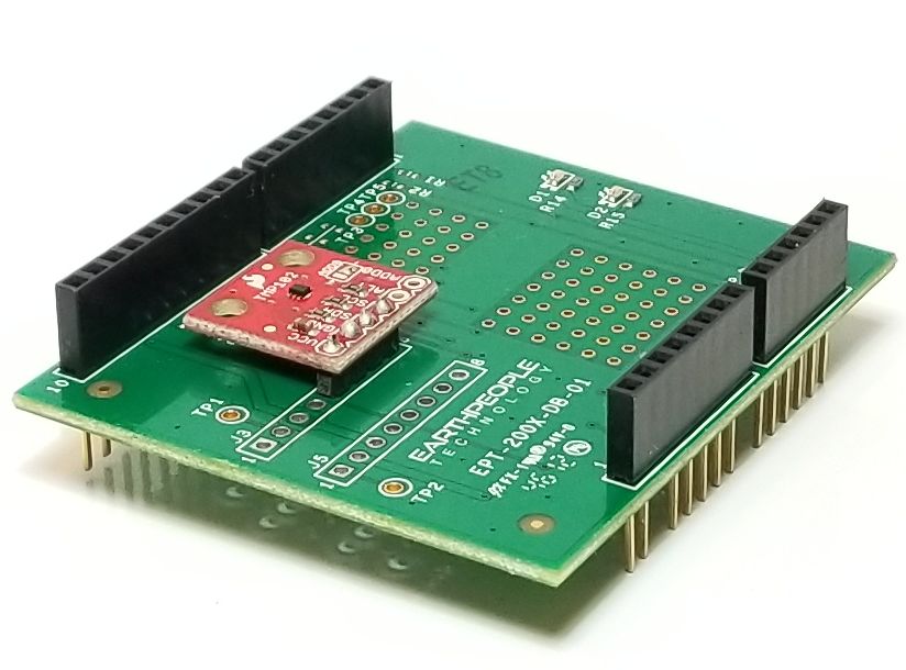
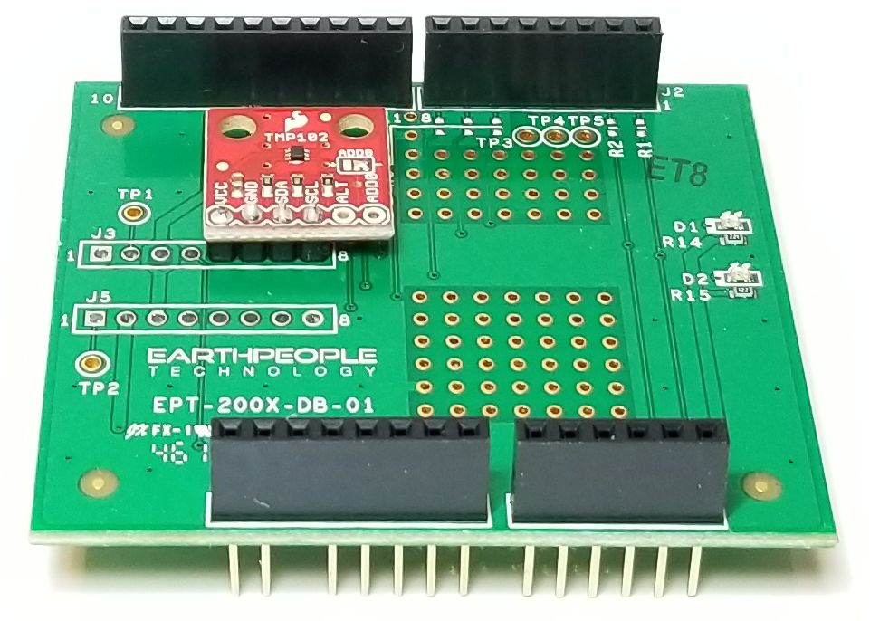
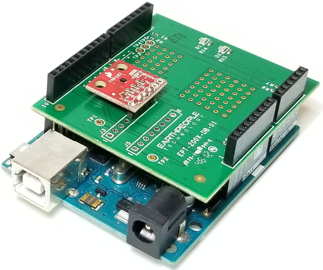
TMP102 Uno Docking Board
TMP102 TEMPERATURE SENSOR
DOCKING BOARD
The TMP102 Temperature Sensor Docking Board
Quickly and easily connects the TMP102 to
the Arduino Uno platform
| The EPT-200TMP-TS-U2 is a temperature sensor mounted on a docking board. The board is designed to fit onto the Arduino Uno platform. It is compatible with the +5V Arduino’s and requires no external hook wires. Just plug the EPT-200TMP-TS-U2 into the Arduino and load the code. The TMP102 temperature sensor power and communications are provided by the docking board connectors from the Arduino. |
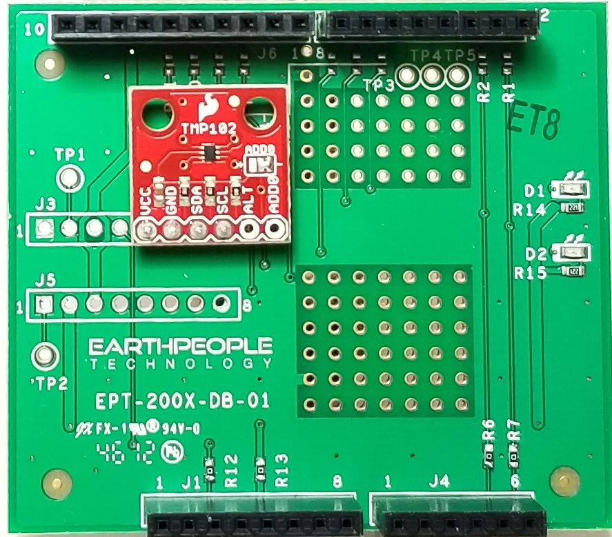
| The EPT-200TMP-TS-U2 is designed for applications that require a robust connection between the sensor and the Arduino platform. These are applications where a bread board and hook up wires could fail. Applications where the boards are subject to vibrations such as robots or industrial environments. The EPT-200TMP-TS-U2 sensor and docking board provides a tight coupling of the board to the Arduino platform. |
Hardware Features:
|
| This docking board is based on the TMP102 Temperature Sensor chip from Texas Instruments. It can measure the ambient temperature between -25℃ to +85℃. The temperature is measured with an accuracy of ± 2.0℃ across the temperature range. The TMP102 is capable of reading temperatures to a resolution of 0.0625°C The docking board provides a robust method (also convenient for connections) to connect the TMP102 to an array of Arduino boards. It is compatible with both +3.3V and +5V Arduinos. There is a power indicator Green LED, and a user Green LED. It has stackable Headers that allow the board to plug into an Arduino and allow other boards to stack on top of it. |

| Coding the Arduino to measure the temperature from the TMP102 is made quite easy using the “Wire” library. All functions required to communicate with the sensor are included in the library. This docking board can be set up and displaying temperature in only a few minutes. See the TMP102 Temperature Sensor Docking Board Project DVD below for an Arduino sketch that is complete and ready to take measurements. |
Downloads
| 85-000010 | TMP102 Temperature Sensor Docking Board User Manual | TMP102_TEMP_DOCK_UM.pdf |
| 95-000010 | TMP102 Temperature Sensor Docking Board Data Sheet | TMP102_TEMP_DOCK_DS.pdf |
| 45-000010 | TMP102 Temperature Sensor Docking Board Project DVD | TMP102_TEMP_SENSOR_PROJECT_DVD |
| 55-000010 | TMP102 Temperature Sensor Docking Board Schematics | EPT_200TMP_TS_U2_SCHEMATICS.PDF |
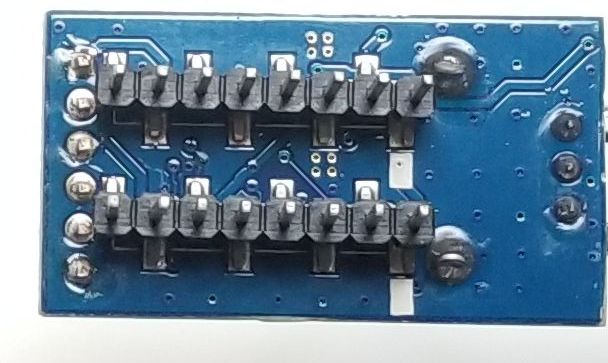
EPT-4901-DA-S1 DAC Board

Purchase at these webstores:
The DSO 100M is a Complete Open
Source Digital Storage Oscilloscope
Development System. It Includes
Four Channels of Analog Input With
a Dedicated 80 MHz Sampling Rate
per Channel
| The Earth People Technology DSO 100M development system is a fully functional USB Digital Storage Oscilloscope. It was designed to be open, flexible and easy to modify. This Open Source Development System allows the user to understand the basics of the typical DSO. All source code along with compiled projects are made available. The user can modify the Verilog code in the FPGA as well as the C# project known as the UnoProlyzer. |
EPT-4901-DA-S1 DAC Board
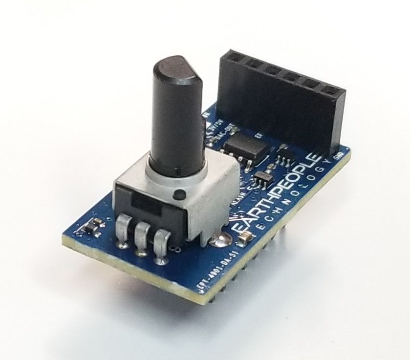
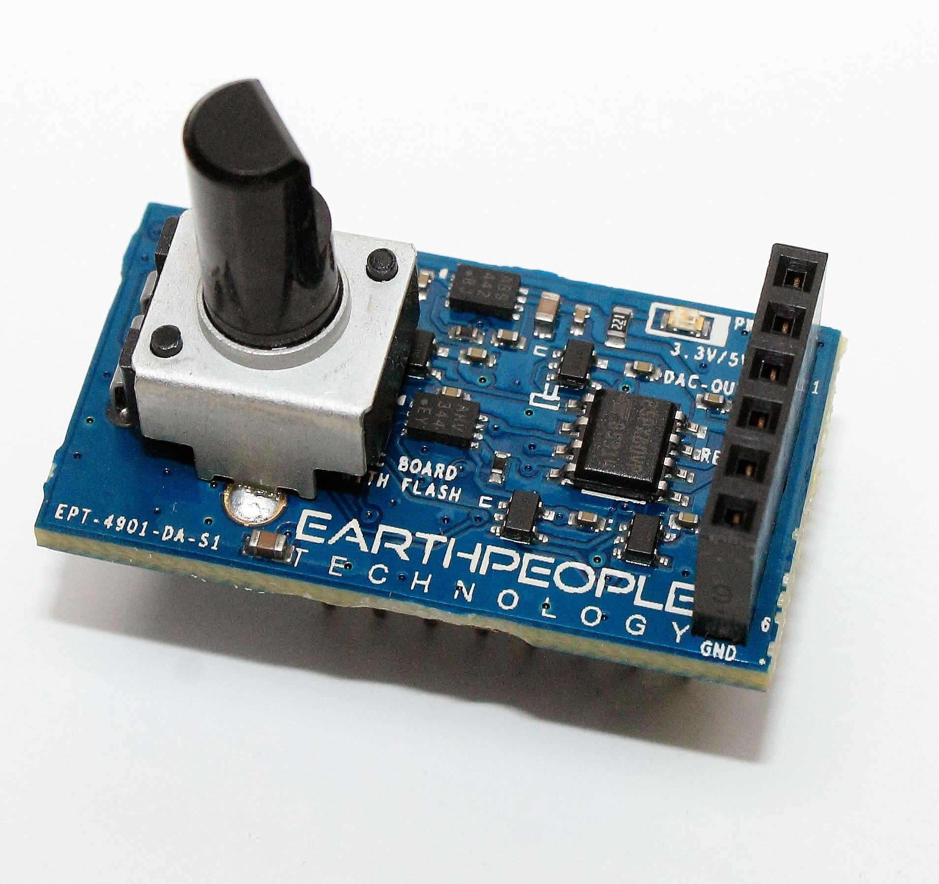
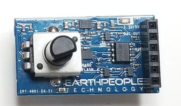
EPT-4901-DA-S1
Digital To Analog Converter Board
The EPT-4901-DA-S1 is an easy to use
DAC Board. It includes
an eight bit DAC and convinient
Bread Board connections
Purchase at these webstores:
| This DAC board features the MCP4091 Eight bit Digital to Analog chip. It is designed to fit into a bread board and connect to any Arduino board. The chip operates from a single 2.7V to 5.5V supply with an SPI compatible Serial Peripheral Interface. So, it can accommodate the +3.3V and +5V Arduinos such as the Mini, Mini Pro, Nano. |

Hardware Features:
|
| The EPT-4901-DA-S1 contains a MCP4091 DAC chip. The board can be used to generate any analog voltage from ground to VREF. VREF is determined by a voltage divider using a potentiometer. The potentiometer allows VREF to vary from zero volts to VCC. VCC is determined by the voltage used to power the EPT-4901-DA-S1. The DAC will accept any input digital value from zero to 255 and convert this value to analog. However, VREF determines the step size of each digital value. |
Digital to Analog Converter
| The MCP4901 is a single channel 8-bit buffered voltage output Digital-to-Analog Converter (DAC). The devices operate from a single 2.7V to 5.5V supply with an SPI compatible Serial Peripheral Interface. The user can configure the full-scale range of the device to be VREF or 2*VREF by setting the gain selection option bit (gain of 1 of 2). The device be can shut down by setting the Configuration Register bit. In Shutdown mode, most of the internal circuits are turned off for power savings, and the output amplifier is configured to present a known high resistance output load (500 kΩ typical). The device include double-buffered registers, allowing synchronous updates of the DAC output using the LDAC pin. These devices also incorporate a Power-on Reset (POR) circuit to ensure reliable powerup. The device utilizes a resistive string architecture, with its inherent advantages of low Differential Non-Linearity (DNL) error and fast settling time. This device is specified over the extended temperature range (+125°C). |
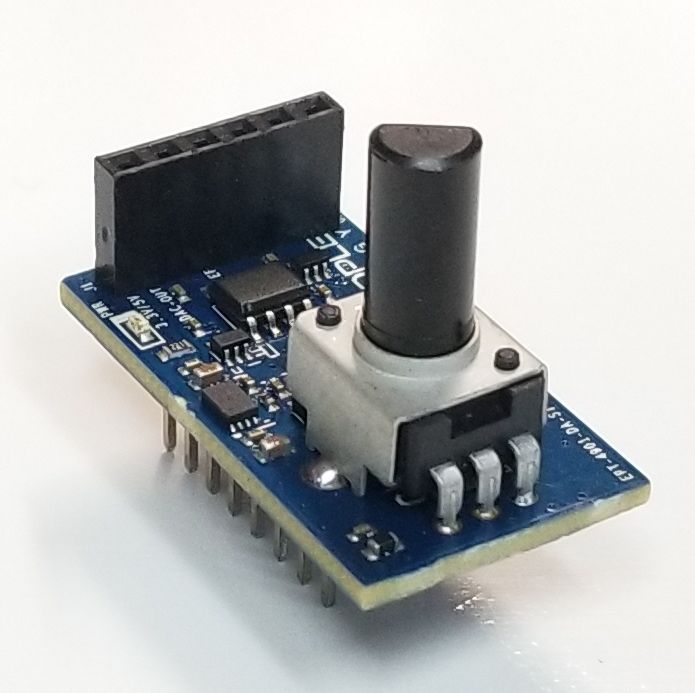
VREF Potentiometer
| The EPT-4901-DA-S1 board includes a 20K potentiometer. This pot forms a voltage divider with a second resistor to vary the voltage applied to VREF. This varied voltage provides an amplitude control for the Analog Out voltage. |
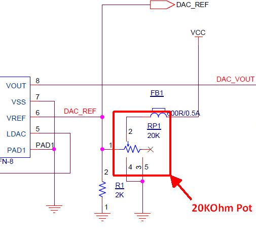
| By varying the VREF, the accuracy of the DAC can be improved. This is because the analog output step size between each DAC digital word is reduced. For example, if the VREF is set to 5V, the analog output step size is 5V/256 (Digital Steps) = 0.0195V per step. If the VREF is set to 2.5V, the analog output step size is 2.5V/256 (Digital Steps) = 0.00976V per step. The smaller the analog step size (or quanta), the more accurate the analog signal can be. |
Downloads
| 85-000010 | MCP4901 Digital To Analog Converter Board User Manual | EPT_4901_DAC_UM.pdf |
| 95-000010 | MCP4901 Digital To Analog Converter Board Data Sheet | EPT_4901_DAC_DS.pdf |
| 45-000010 | MCP4901 Digital To Analog Converter Board Project DVD | EPT-4901-DAC-PROPJECT_DVD |
| 55-000010 | MCP4901 Digital To Analog Converter Board Schematics | EPT_4901_DA_SCHEMATICS.PDF |
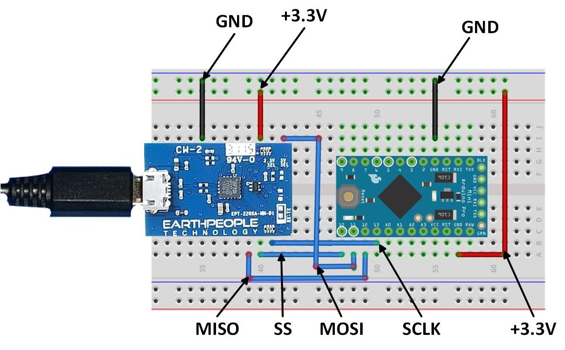
USB SPI Slave Breakout Board
 USB SPI Slave Breakout Board
Transfer SPI data directly to the PCThe USB SPI Slave Breakout Board provides a simple interface for bi-directional communication with the PC from any MCU (including the Arduino family). It is designed to connect directly to the standard bread board with a reduced footprint. Once connected to an MCU, the MCU Master SPI bus connects to the FT220X chip. This chip connects the SPI bus to the USB bus. The PC communicates with the USB SPI Slave Breakout Board as COM Port. This allows any simple Terminal Window software (such as TeraTerm) to communicate directly with the MCU. Earth People provides sample software so the user can use the Arduino functions to send data to be graphed on the PC. |
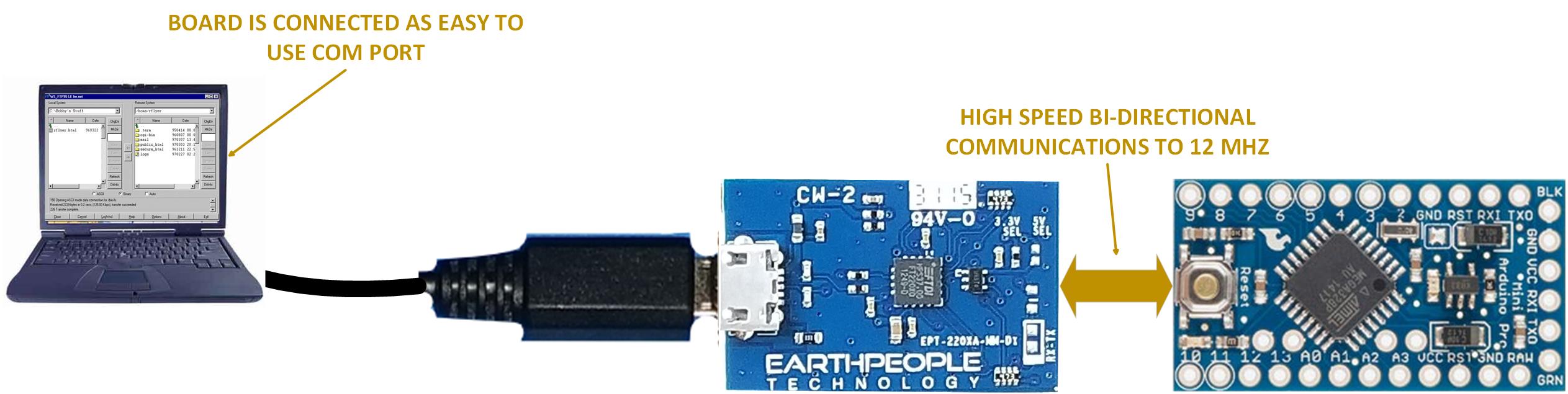
Hardware Features:
- USB 2.0 Full Speed
- Independent USB to SPI Slave Bus Running 12MHz Max Clock Speed
- Board is used as COM Port on the PC
- USB Powered
- Provides external +3.3volts @ 50mA
- FT220X FTDI chip has on chip 512 byte Receive and Transmit Buffers
- Compatible with any external +5/3.3 Volt MCU (Including all Arduinos)
Description
| The USB SPI Slave Breakout Board consists of the FT220X chip from FTDI. This single chip solution connects the Slave SPI bus directly to USB. The board includes a USB Micro B connector and two 1×8 0.1 inch headers. The board is powered from the USB port of the PC. It provides +3.3V regulated output to power up user MCU’s or any other power need. Current from the +3.3V regulated output is 50mA. No external power is needed for the USB SPI Slave Breakout Board. |

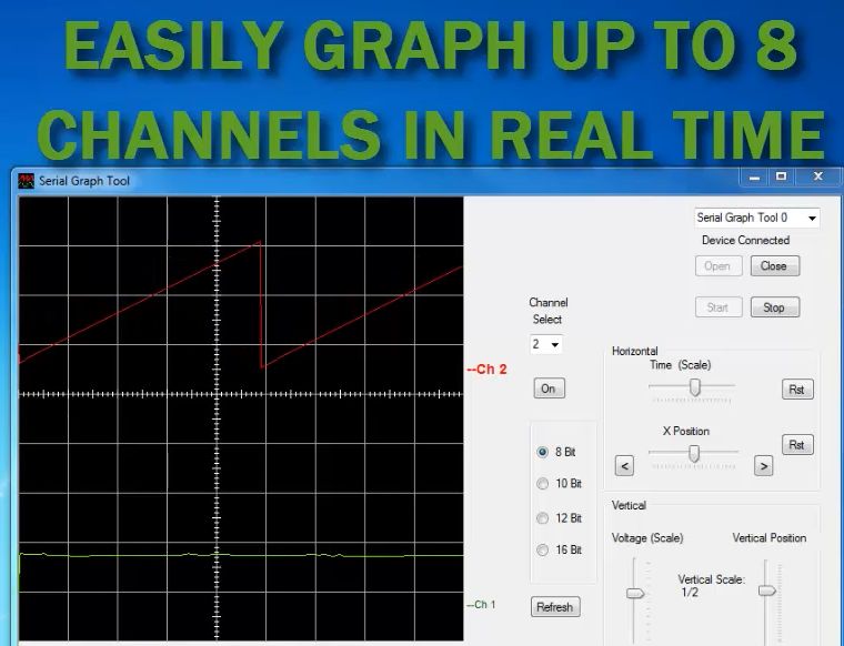
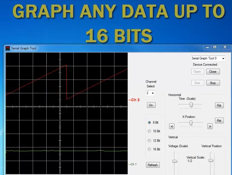
High Speed Data Display
| The USB SPI Slave Breakout Board comes with example software that displays data from the External MCU (Such as the Arduino Mini Pro). The user can display multiple channels of data analog, temperature sensor or digitally generated data. |
Downloads
| 85-000040 | USB SPI Slave Breakout Board User Manual | USB_SPI_SLAVE_BREAKOUT_BOARD_UM.pdf |
| 95-000040 | USB SPI Slave Breakout Board DataSheet | USB_SPI_SLAVE_BREAKOUT_BOARDL_DS.pdf |
| 45-000040 | USB SPI Slave Breakout Board Projects DVD | USB_SLAVE_SPI_BREAKOUT_PROJECT_3.0_DVD.ZIP |
| 55-000040 | USB SPI Slave Breakout Board Schematics | USB_SPI_SLAVE_BREAKOUT_SCHEMATICS.PDF |
| 35-000001 | EPT Drivers | EPT_2.12.00.exe |
TMP102 Temperature Sensor Breakout Board
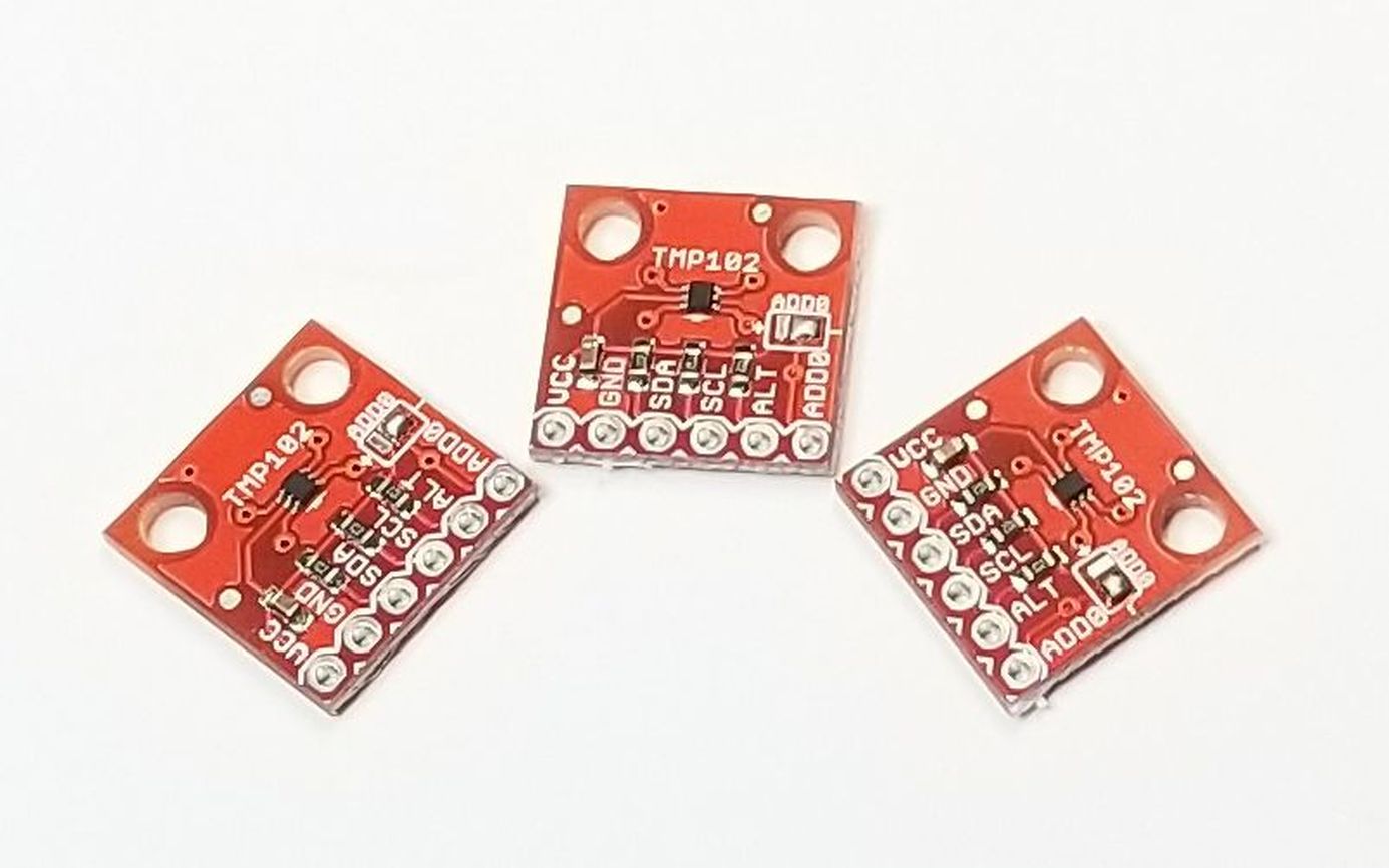

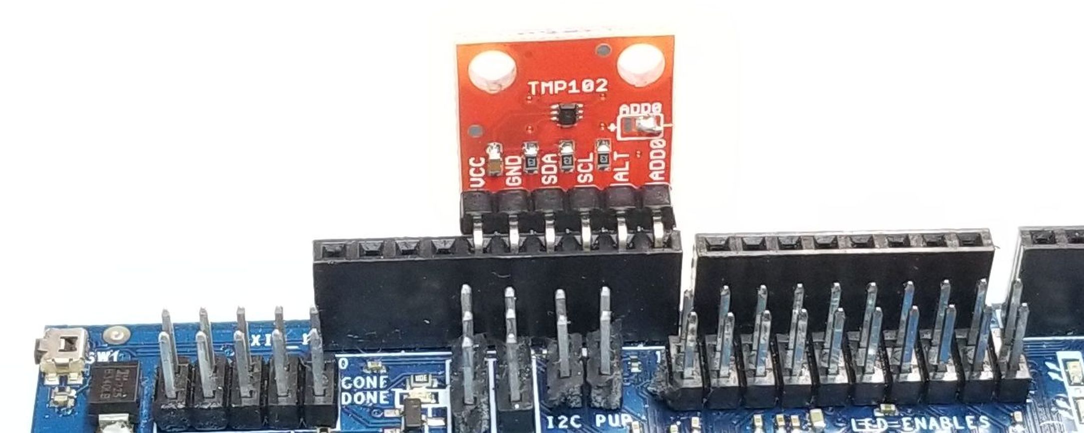
TMP102 TEMPERATURE SENSOR
BREAKOUT BOARD
The TMP102 Temperature Sensor Breakout Board
Quickly and easily connects the TMP102 to
the Arduino Uno platform
| The EPT-TMP102-BD-S8 is a temperature sensor mounted on a breakout board. The board is designed to fit onto the Arduino platform. It is compatible with the +5V Arduino’s and can also connect to +3.3V boards. Just wire the EPT-200TMP-TS-U2 into the Arduino and load the code. The TMP102 temperature sensor power and communications can be provided by the board connectors from the Arduino. |
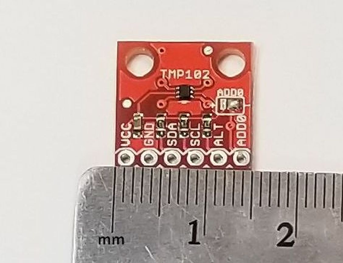
Hardware Features:
|
| This breakout board is based on the TMP102 Temperature Sensor chip from Texas Instruments. It can measure the ambient temperature between -25℃ to +85℃. The temperature is measured with an accuracy of ± 2.0℃ across the temperature range. The TMP102 is capable of reading temperatures to a resolution of 0.0625°C The board provides a convenient connection, via the I2C interface, |

| Coding the Arduino to measure the temperature from the TMP102 is made quite easy using the “Wire” library. All functions required to communicate with the sensor are included in the library. This docking board can be set up and displaying temperature in only a few minutes. See the TMP102 Temperature Sensor Breakout Board Project DVD below for an Arduino sketch that is complete and ready to take measurements. |
Downloads
| 85-000010 | TMP102 Temperature Sensor Breakout Board User Manual | TMP102_TEMP_DOCK_UM.pdf |
| 95-000010 | TMP102 Temperature Sensor Breakout Board Data Sheet | TMP102_TEMP_DOCK_DS.pdf |
| 45-000010 | TMP102 Temperature Sensor Breakout Board Project DVD | TMP102_TEMP_SENSOR_PROJECT_DVD |
| 55-000010 | TMP102 Temperature Sensor Breakout Board Schematics |
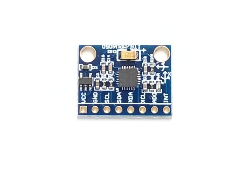
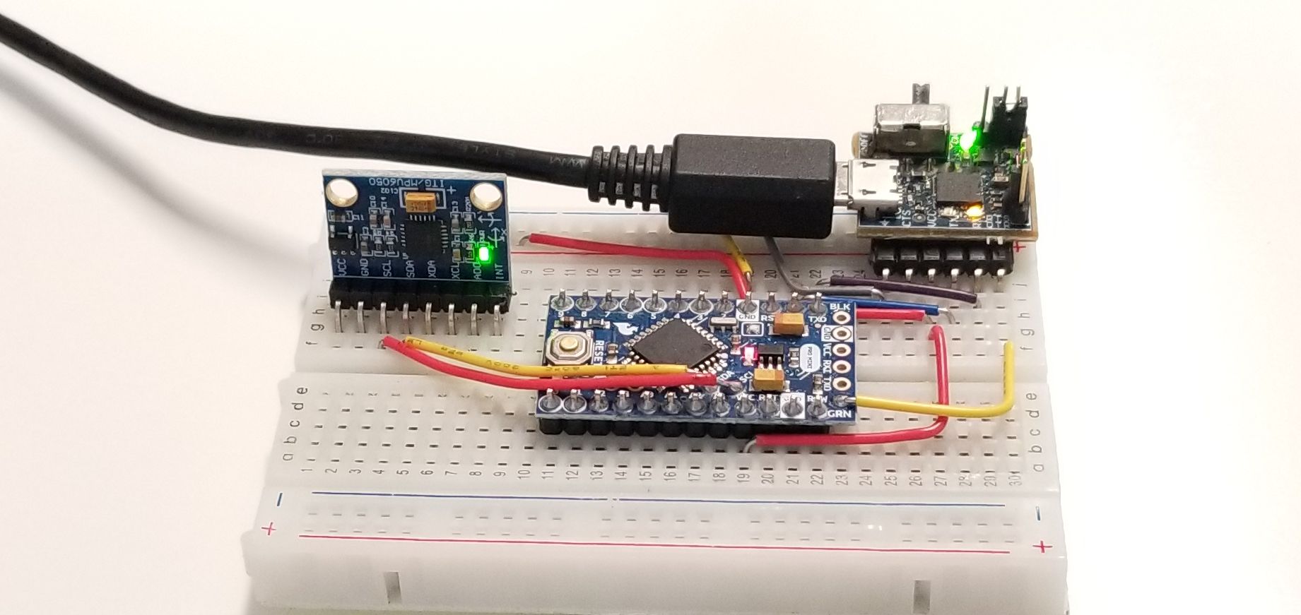
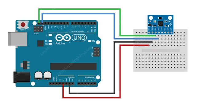
MPU-6050 Breakout Board

TRIPLE AXIS ACCELEROMETER AND GYRO BREAKOUT BOARD
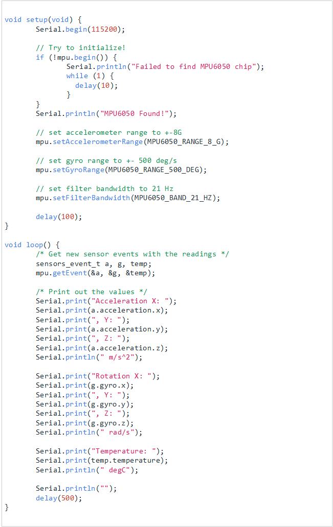
| This breakout board allows you to use your MPU6050 Accelerometer/Gyroscope sensors with any MCU including the Arduino platform. It is compatible with the +5V Arduino’s and can also connect to +3.3V boards. Just wire the EPT-M6050-BD-S8 into the Arduino and load the code. The I²C Bus is required to be set up in your configuration for this sensor to work. |
6-axis MotionProcessing™ solution
|
The MPU-6000™ family provides the world’s first integrated 6-axis MotionProcessing™ solution that eliminates the package-level gyro/accel cross-axis misalignment associated with discrete solutions. The devices combine a 3-axis gyroscope and a 3-axis accelerometer on the same silicon die together with an onboard Digital Motion Processor™ capable of processing complex 9-axis MotionFusion algorithms. The parts’ integrated 9-axis MotionFusion algorithms access external magnetometers or other sensors through an auxiliary master I2C bus, allowing the devices to gather a full set of sensor data without intervention from the system processor. The devices are offered in the same 4x4x0.9 mm QFN footprint and pinout as the current MPU-3000™ family of integrated 3-axis gyroscopes, providing a simple upgrade path and making it easy to fit on space constrained boards. |

Hardware Features:
|
Easily Code up the Accel/Gyro
| Coding the Arduino to measure movement using the MPU-6050 is made quite easy using the “Wire” library. All functions required to communicate with the sensor are included in the library. This board can be set up and displaying movement in only a few minutes. See the MPU-6050 Gyro and Accelerometer Sensor Breakout Board Project DVD below for an Arduino sketch that is complete and ready to take measurements. |
Downloads
| 85-000010 | MPU-6050 Accelerometer and Gyro Breakout Board User Manual | MPU6050_BREAKOUT_UM.pdf |
| 95-000010 | MPU-6050 Accelerometer and Gyro Breakout Board Data Sheet | MPU6050_BREAKOUT_DS.pdf |
| 45-000010 | MPU-6050 Accelerometer and Gyro Breakout Board Project DVD | MPU6050_BREAKOUT_PROJECT_DVD |
| 55-000010 | MPU-6050 Accelerometer and Gyro Breakout Board Schematics | EPT_M6050_BD_S8_V1.pdf |
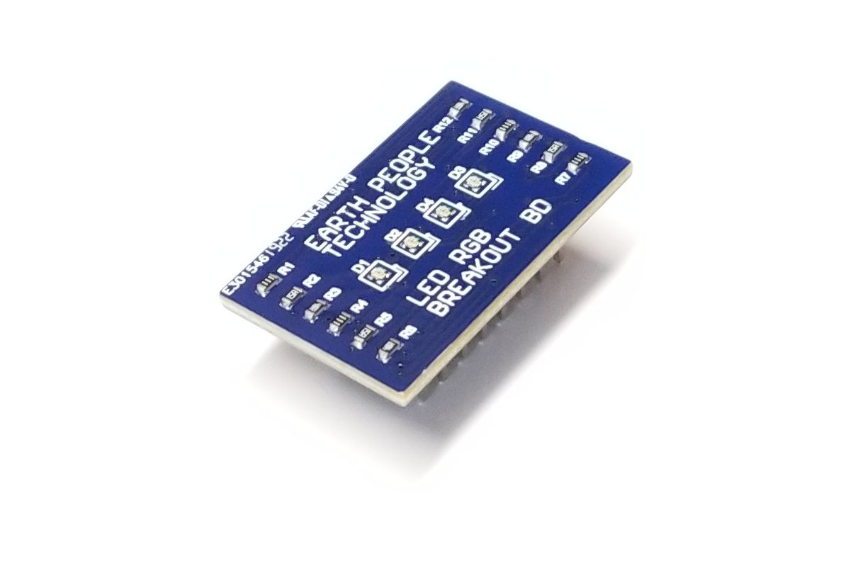
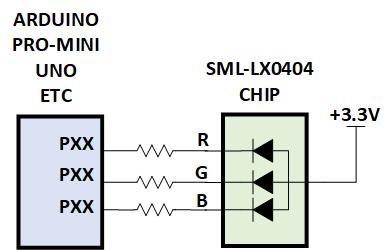
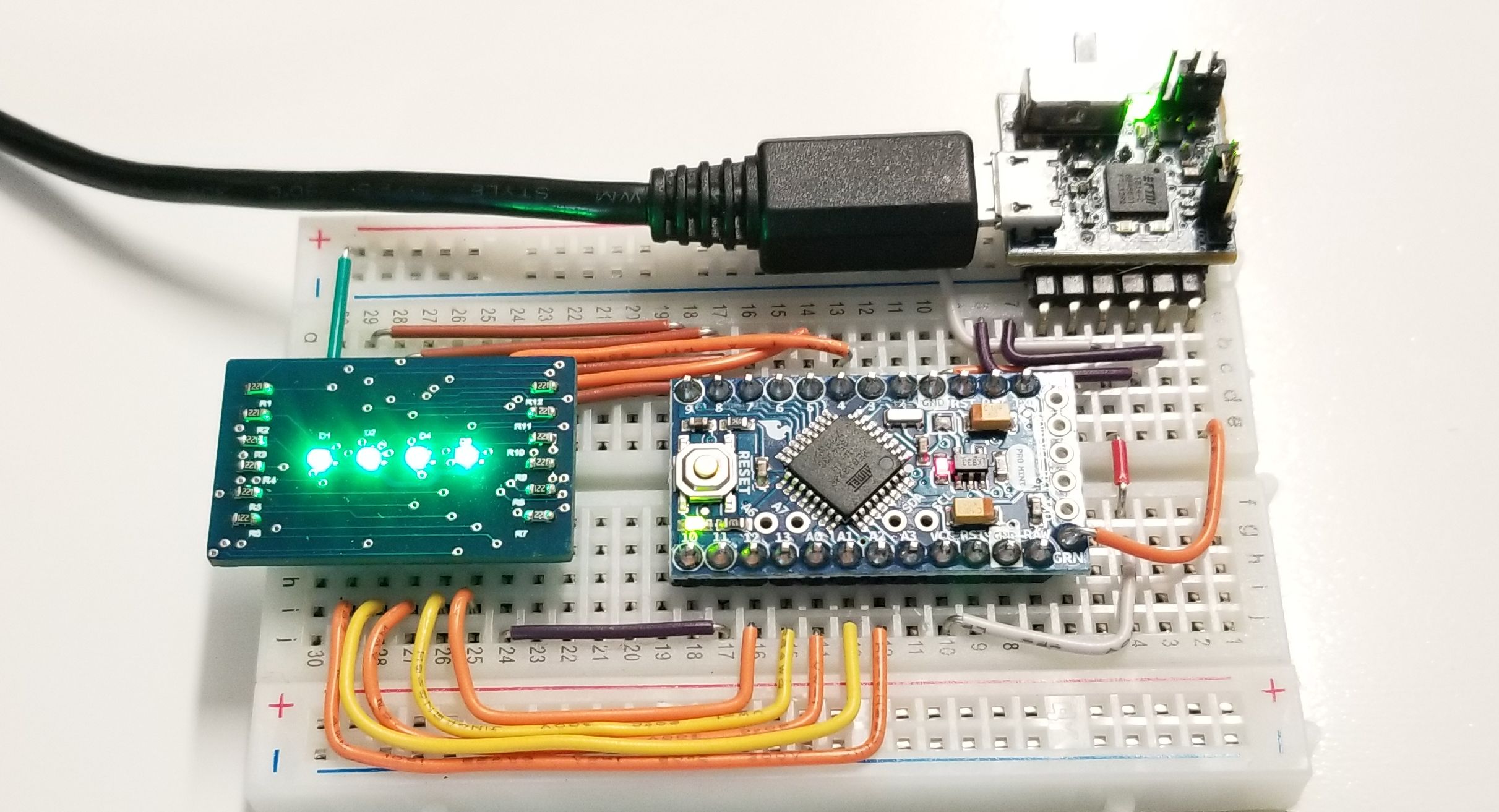
LED RGB Breakout Board

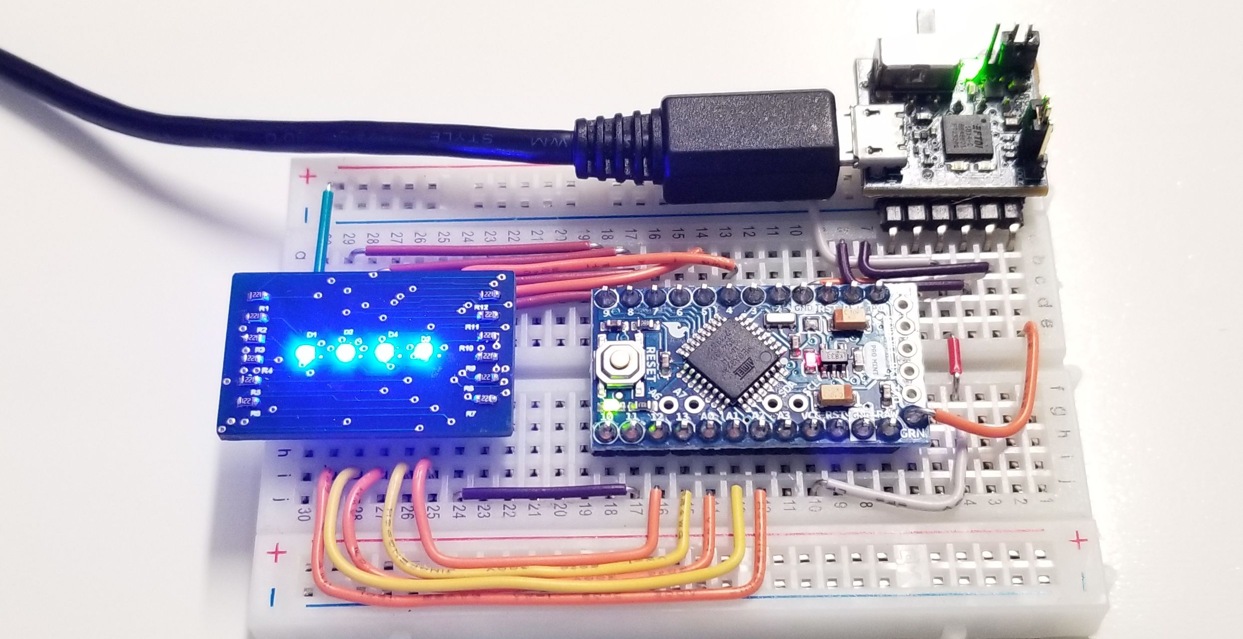 LED RGB Breakout Board
SML-LX0404 LED RGB Breakout BoardThe LED RGB Breakout Board provides a simple interface to control four LED RGBs for |
Hardware Features:
|
Description
| The LED RGB Breakout Board consists of four Lumex SML-LX0404SIUP LED chips. The SML-LX0404 chip is a current sink and can be connected to any MCU. The anode should be connected to +3.3V. The reason for this is the Series resistors are calculated for current limiting based on +3.3V. Changing the anode voltage to another source will change the brightness emitting from each LED. Because the SML-LX0404 chips are current sink, the user can connect to either +5V or +3.3V Arduino (or other MCUs) and control each LED. |
LED Electrical SpecificationsEach LED current limiting resistor is calculated to provide 5mA in each |
| Parameter | Red LED | Green LED | Blue LED | Units |
|---|---|---|---|---|
| Peak Wavelength | 632 | 518 | 564 | nm |
| Forward Voltage | 1.75 | 2.75 | 2.60 | Volts |
| Leg Current | 5 | 5 | 5 | mA |
| Resistor | 310 | 110 | 140 | Ohms |
| Axial Intensity | 30 | 40 | 20 | mcd |
Earth People provides sample software so the user can use the Arduino functions
to control the LED RGBs. The user can control all aspects of each LEDs on/off time.
Adding pulse width controlled signals to the LEDs
allows a wide variety of colors to be displayed by the LED RGBs.
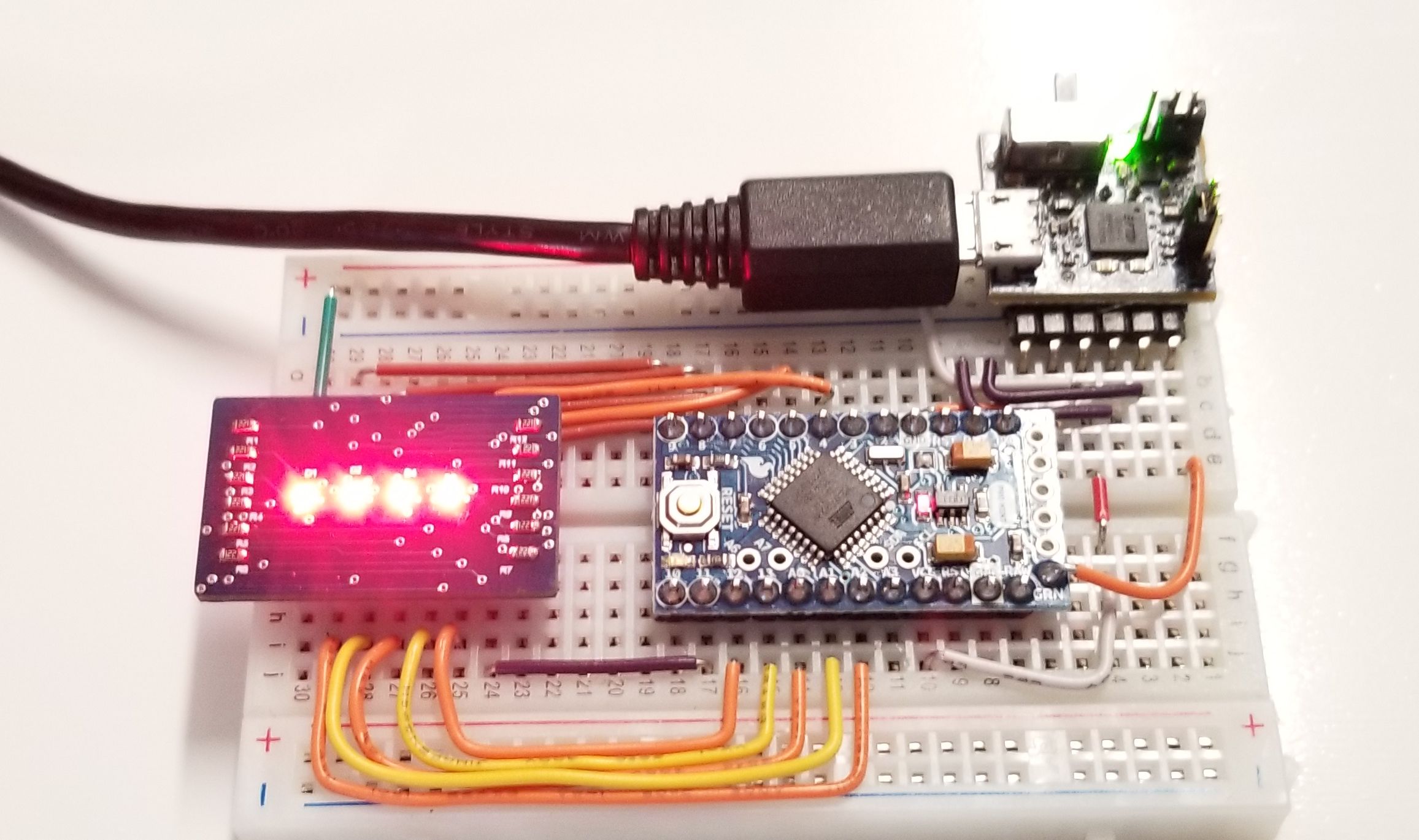
Easily Control four LED RGBs from an Arduino
| The LED RGB Breakout Board comes with example software that blinks individual LEDs from the External MCU (Such as the Arduino Mini Pro). The user can display multiple colors using each LED RGB. The MCU will provide pulse width modulated control for each LED. Changing the duty cycle of each LED changes the overall color of the LED RGB. |
Downloads
| 85-000040 | LED RGB Breakout Board User Manual | LED_RGB_BREAK_OUT_UM_V2.pdf |
| 95-000040 | LED RGB Breakout Board DataSheet | LED_RGB_BREAKOUT_BOARD_DS_V3.pdf |
| 45-000040 | LED RGB Breakout Board Projects DVD | LED_RGB_BREAKOUT_PROJECT_1.0_DVD.ZIP |
| 55-000040 | LED RGB Breakout Board Schematics | LEDRGBV1.3_Schemtic.pdf |
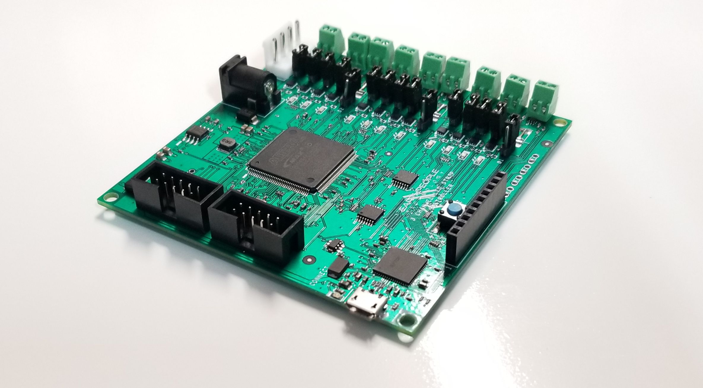
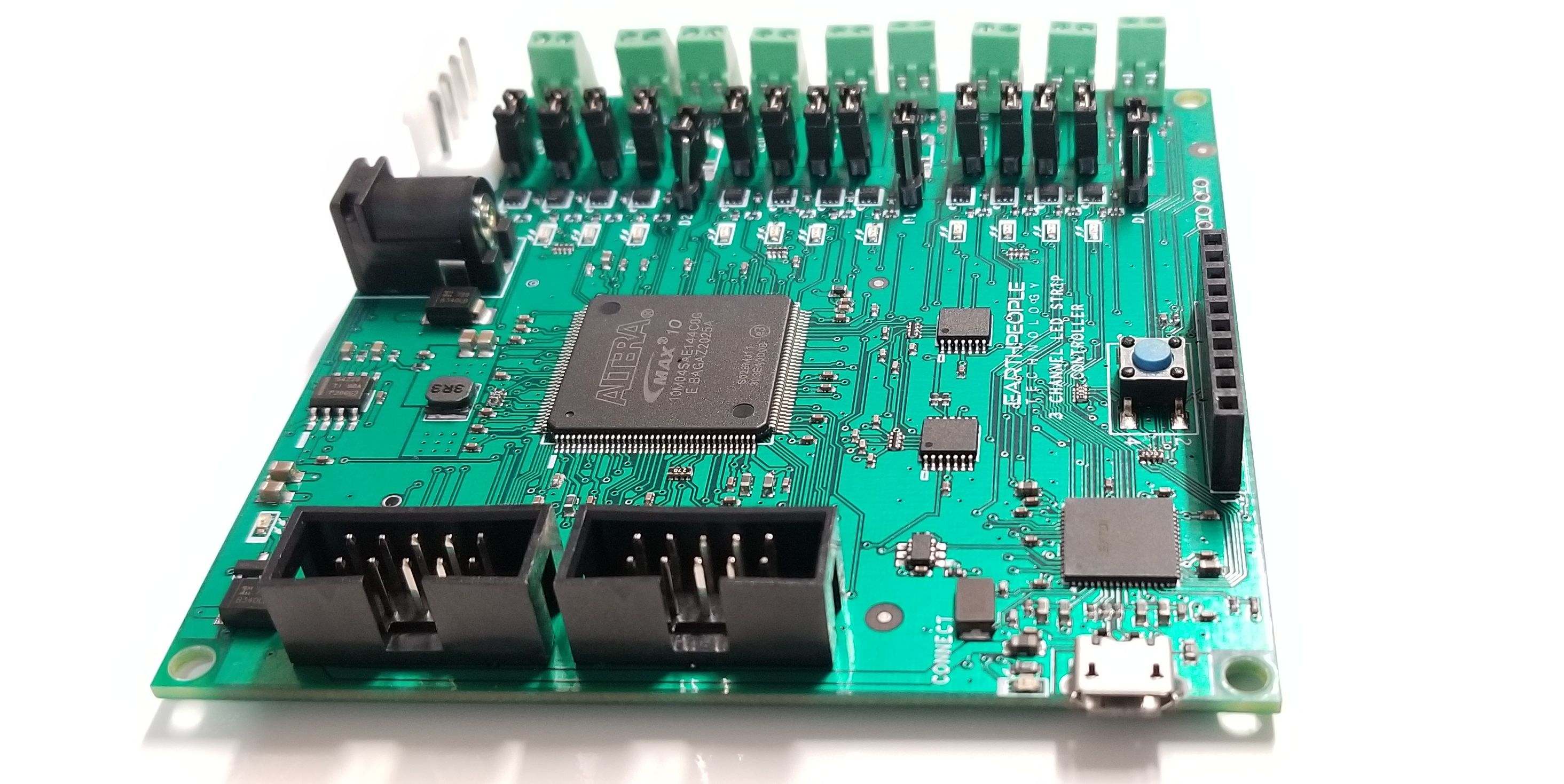
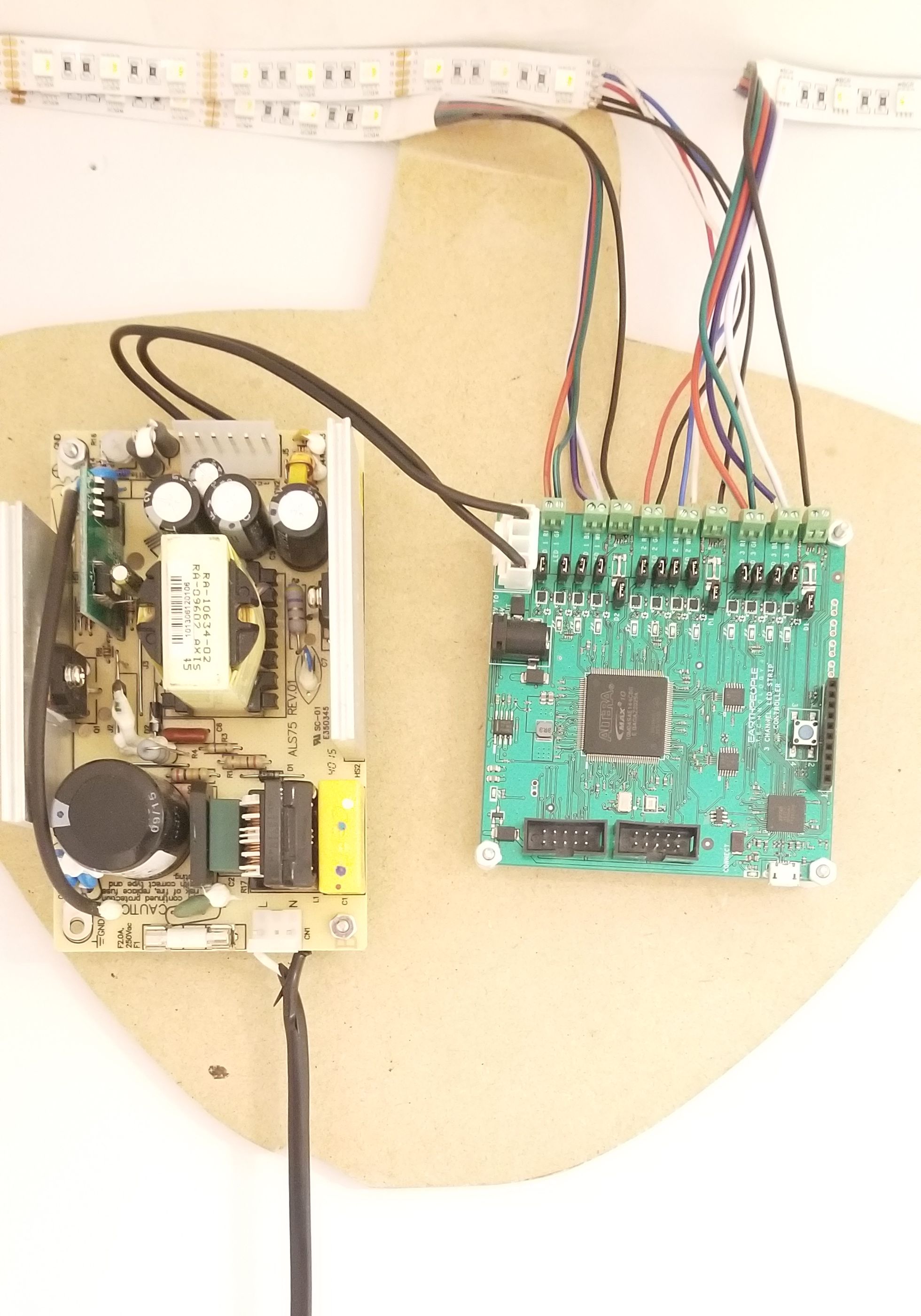
LED Strip Controller Board
 LED Strip Controller Board
| The LED Strip Controller is a board that provides complete control over 12 seperate individual strips. It includes an Intel/Altera MAX10 FPGA. |
| LED Strip Controller |
Control 12 Individual Separate LED Strips
| TLED Strip Controller |

| LED Strip Controller |
LED Strip Projects
| LED Strip Controller |

| LED Strip Controller |
Configuring the FPGA
| LED Strip Controller |
| LED Strip Controller |
Downloads
| 85-000012 | LED Strip Controller User Manual | LED_STRIP_CONTROLLER_UM.pdf |
| 95-000012 | LED Strip Controller Data Sheet | LED_STRIP_CONTROLLER_DS.pdf |
| 45-000012 | LED Strip Controller Project DVD | LED_STRIP_CONTROLLER PROJECT DVD |
| 55-000012 | LED Strip Controller Schematics | LED_STRIP_CONTROLLER-SCHEMATICS.pdf |
| 35-000001 | EPT Drivers | EPT_2.08.24.ZIP |
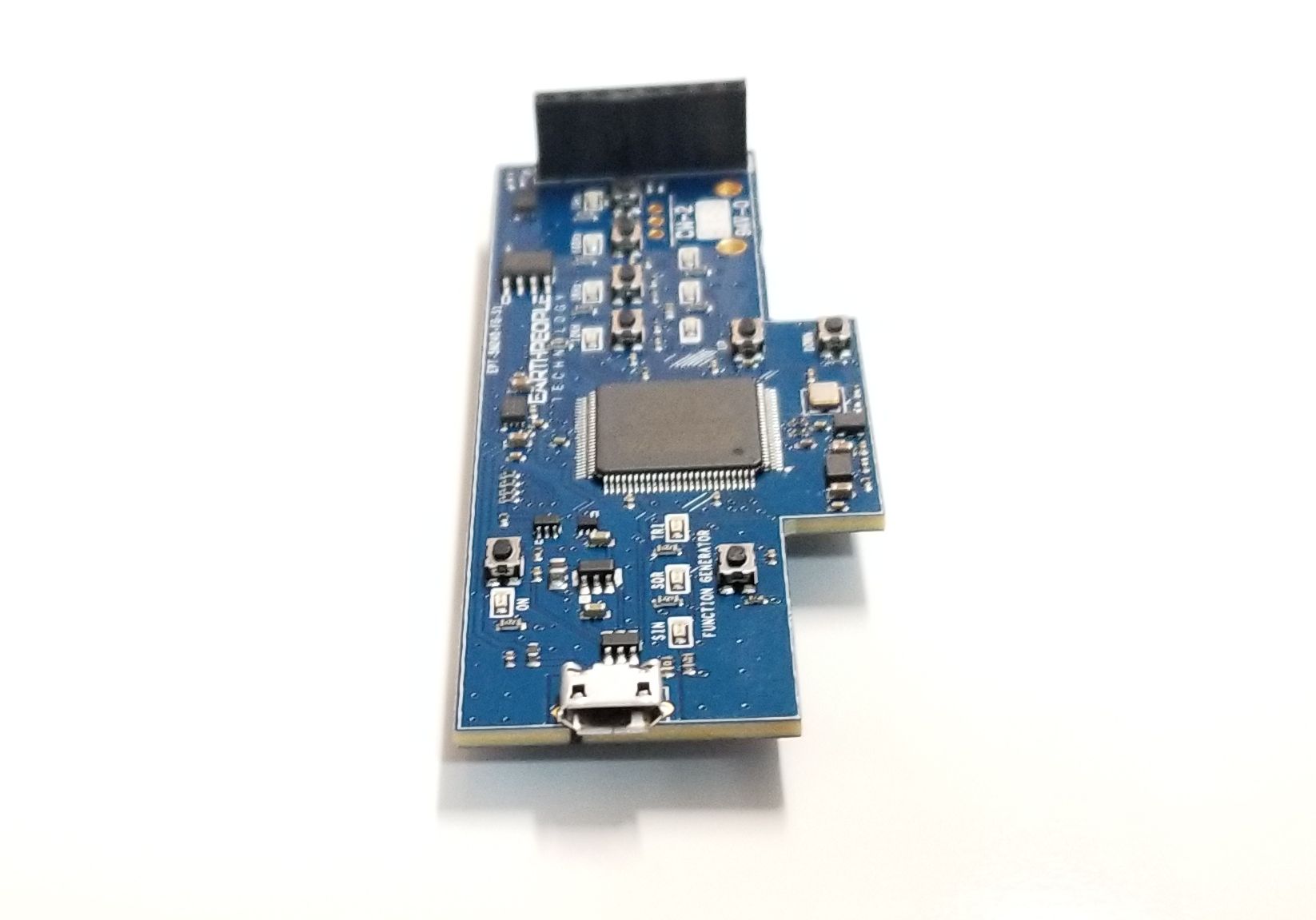
BeeProLogic CPLD Development Board
The BeeProLogic is an Easy To Use
Beginners CPLD Development Board.
BeeProLogic CPLD Development Board
| The BeeProLogic is a CPLD development board that is designed to be user friendly and a great introduction into digital design for Electrical Engineering students and hobbyists. This board provides a simplified method for debugging programmable logic code. It has been designed with plenty of LEDs and Pushbuttons to allow a large amount of interaction between user and hardware operations. |
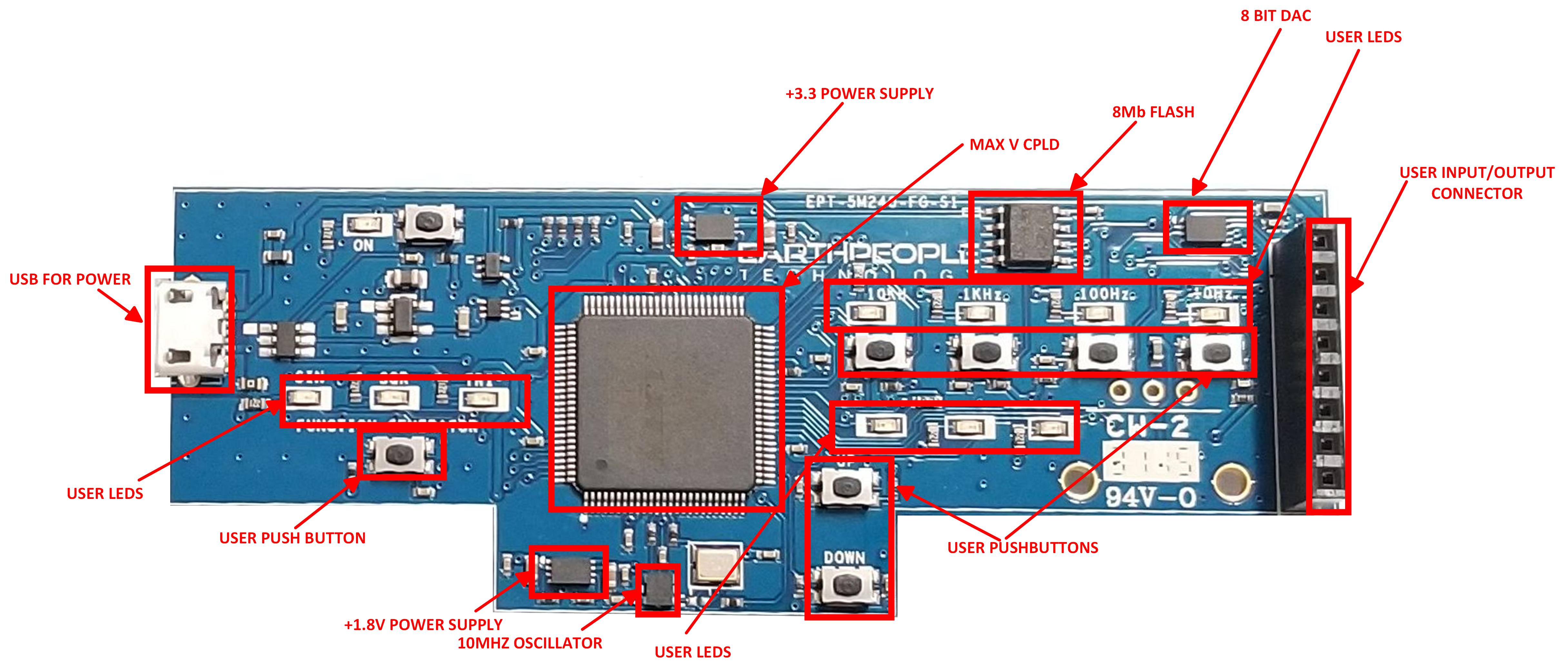
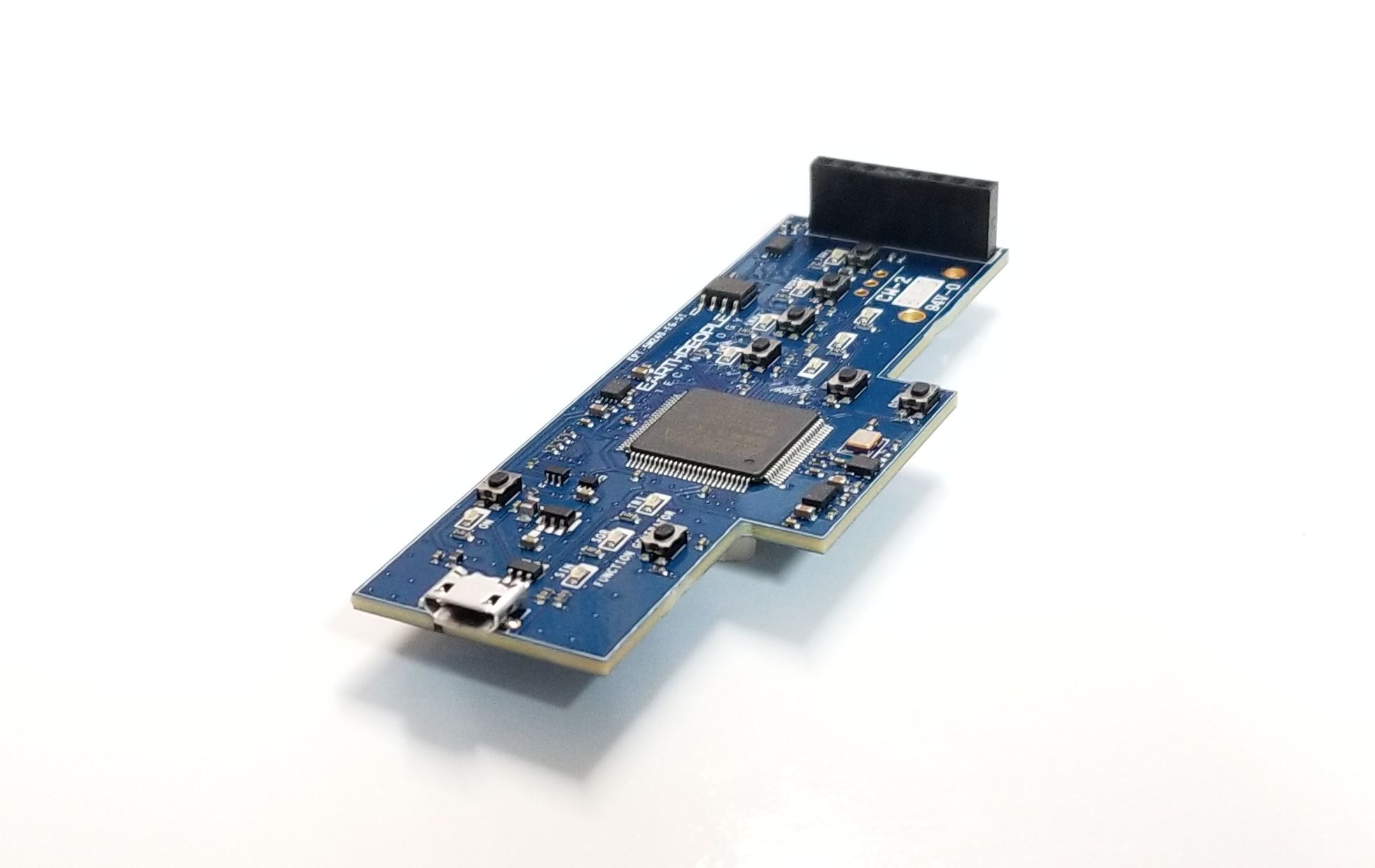
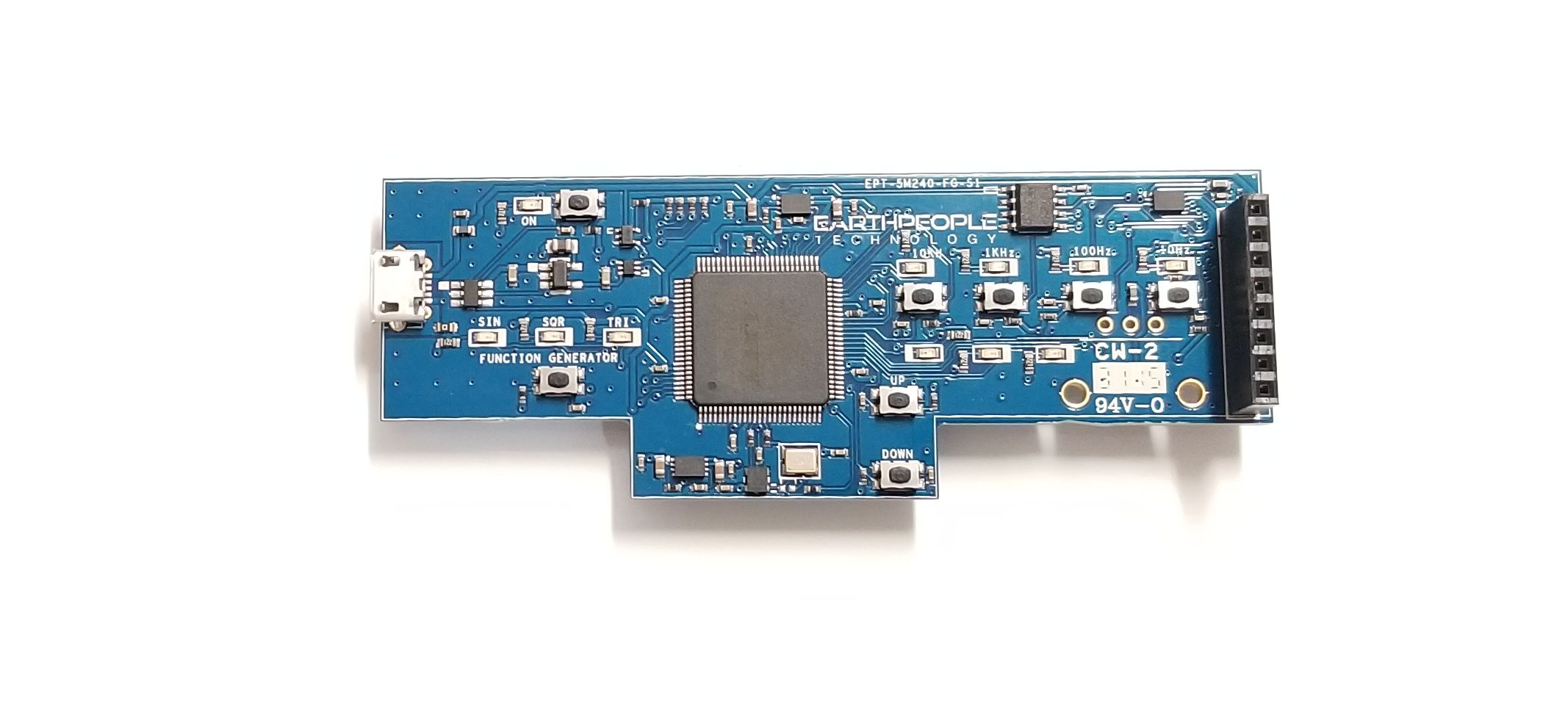
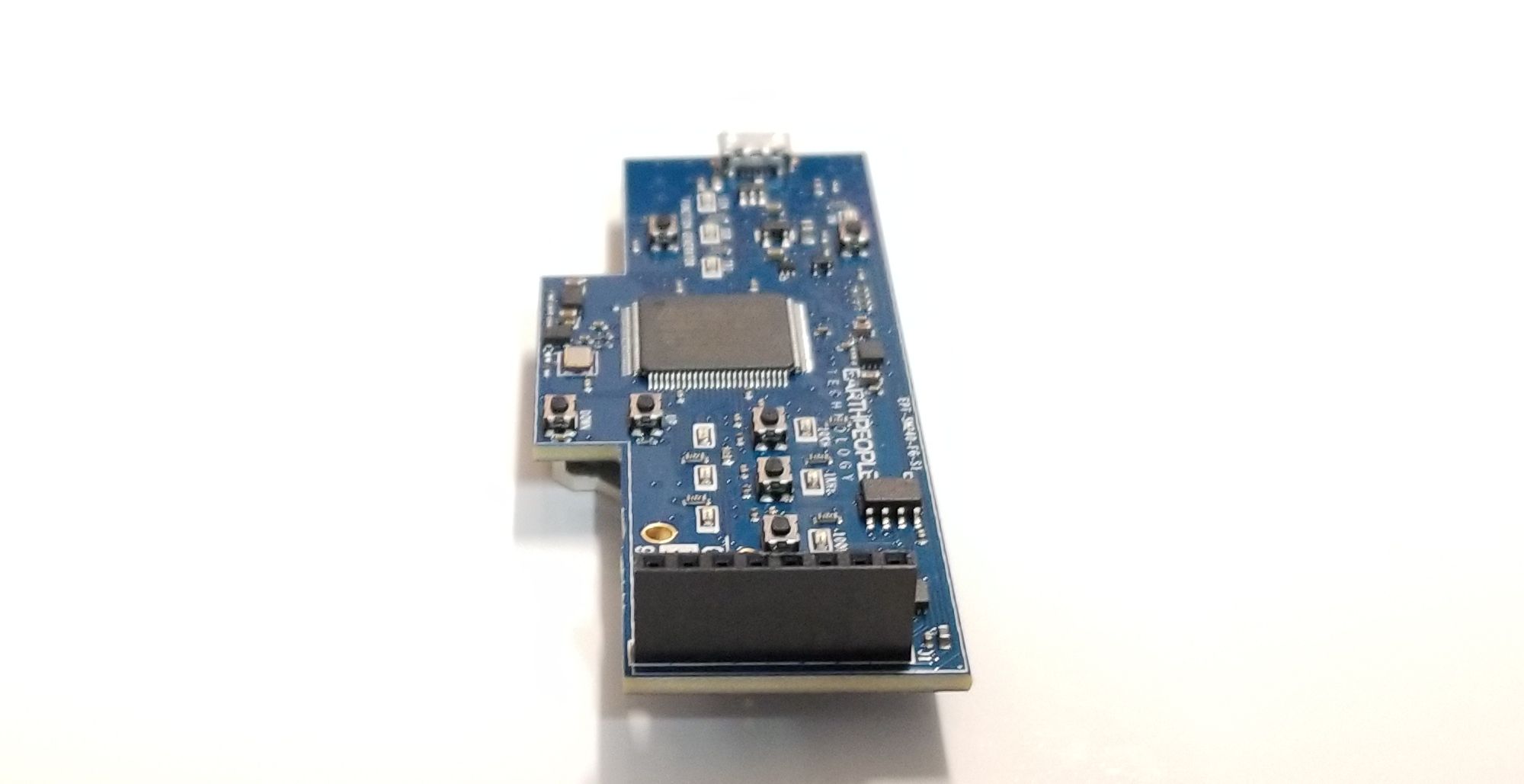
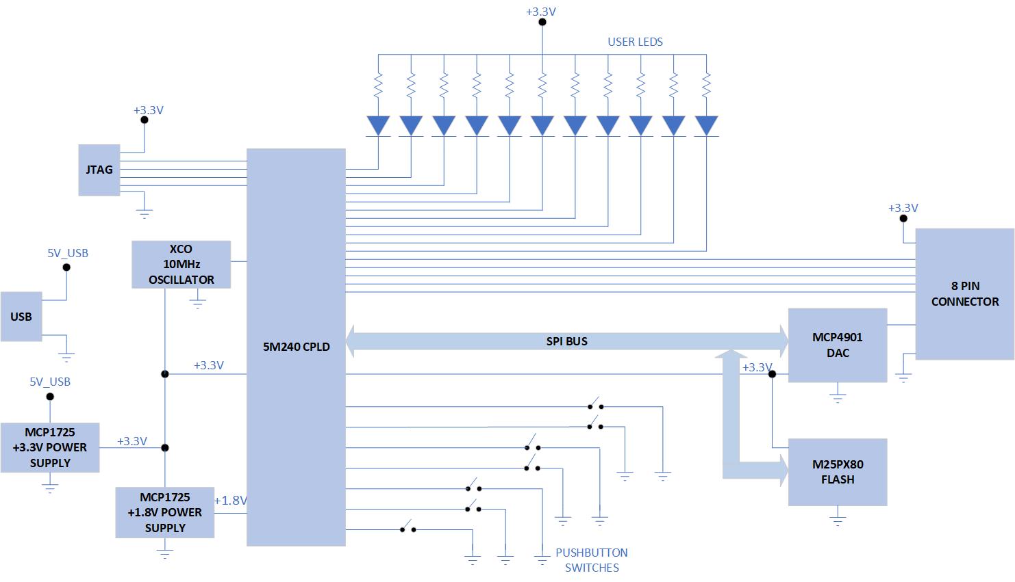
| The Earth People Technology BeeProLogic CPLD development system hardware consists of a a CPLD, 8Mb Flash and a single channel DAC. The board requires an external JTAG Programmer compatible with the JTAG Blaster. The Core of the board is the MAX V chip. The board can be powered by standard USB Micro B connector. There is a 10MHz oscillator attached to the MAX V chip for clocking user code. The board also includes 10 Green User LEDS, Seven User Pushbuttons and One external connector with six pins for GPIO. |
Hardware Features:
|
Simplified Development Board
| The BeeProLogic DVD provides detailed step by step instructions to quickly guide the user to create a project, synthesize the project and download the programming file into the CPLD. The Quartus Prime Software must be downloaded from Intels website. Once the Quartus software is on your desktop, the guide will show you how to create a project, write you first LED blinky code, compile and program the CPLD. |
Programming the BeeProLogic Board
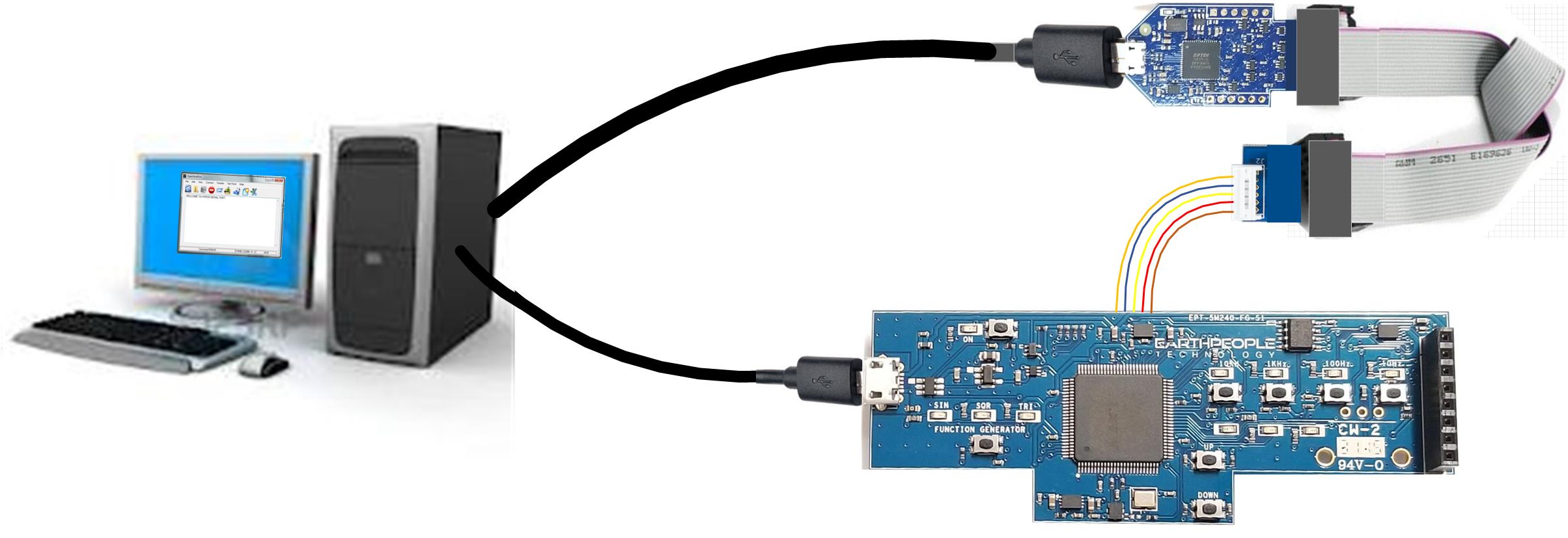
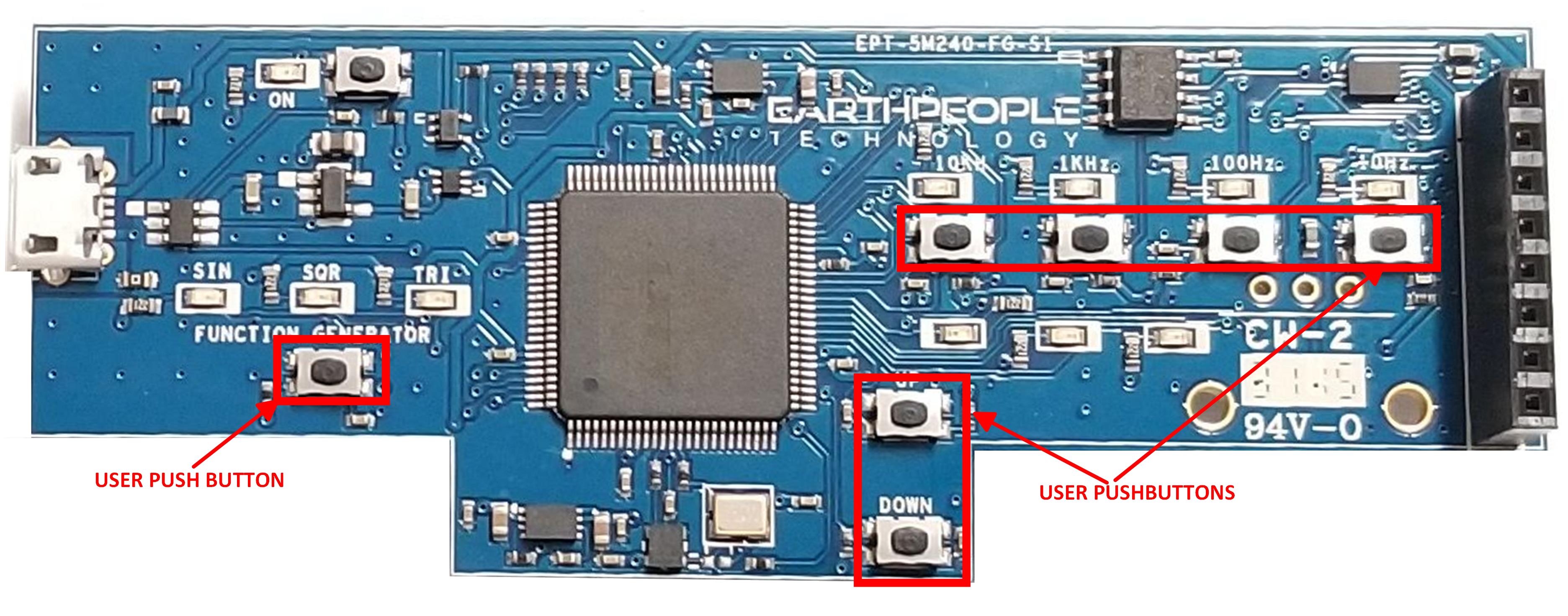
| The CPLD on the BeePro can be programmed with the code created by the user. Programming is quick and easy. The BeeProLogic Does Not Include An OnBoard programmer. The user must purchase a separate JTAG Blaster. To program the board, a standard USB Micro-B cable must be connected from power (USB Port on laptop) to the board. Then connect the JTAG Blaster to a USB Port on a laptop. Use the provided adapter to connect the JTAG Blaster 10 pin connector to the 6 pin. 2mm pitch connector. Connect the 6 pin 2mm pitch connector to the BeeProLogic connector on the back of the board. |
| Use the Quartus Prime Software Tools to program the 5M240 CPLD on board the BeeProLogic. The User Manual includes step by step instructions on building the user project. It includes the steps to successfully program the CPLD. |
Controlling The Board
The User LEDs
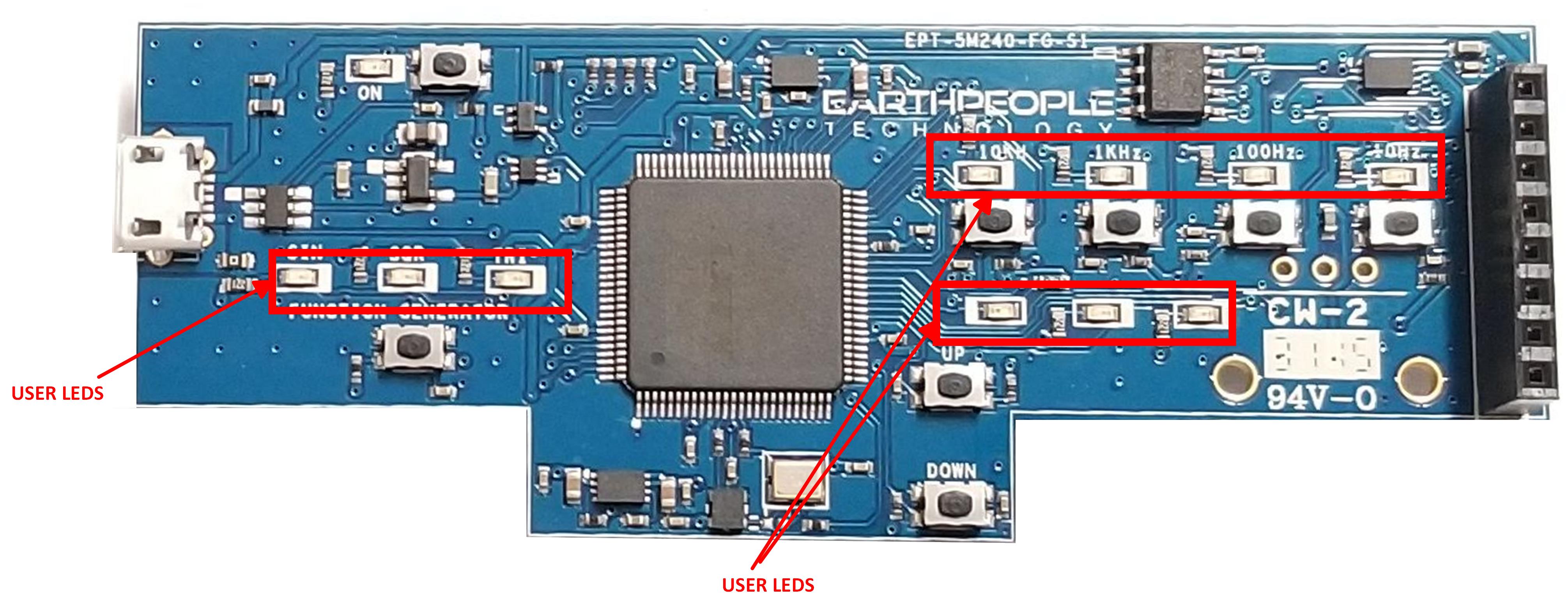
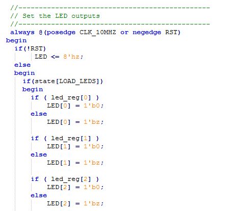
| The BeeProLogic includes eleven user LEDs. The LEDs are directly sinked from the CPLD with the anode connected to +3.3V. This voltage is used to meet the forward voltage along with a 220 Ohm series resistor for each LED. The resistor provides the series current through the LEDS and controls the brightness. |
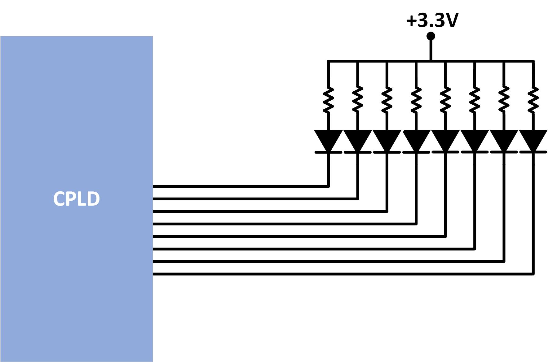
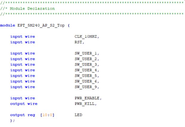
| The code to drive the LEDs is either zero (1’b0) or floating (1’bz). First, declare the LED as an output. In the example below, the vector LED is set to ‘reg’ because it is driven in an always block. |
| To turn the selected LED on, set the signal equal to 1’b0. This will apply a ground to the cathode side of the LED and allow current to flow through the circuit turning the LED on. To turn the selected LED off, set the signal equal to 1’bz. This will float the cathode side of the LED and no current will flow through the LED. |
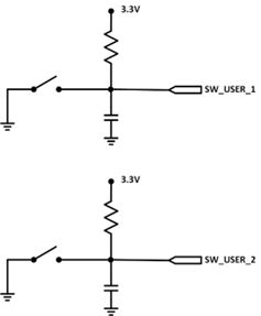
The User Pushbuttons
| The BeeProLogic includes eight push button switches. All are momentary contact switches. They include a 1uF cap to ground to debounce both switches. The code to use these switches is simple, just declare an input on the selected switch pin. Then use code to activate the a function with the input signal goes to low. |
The 8 Bit DAC
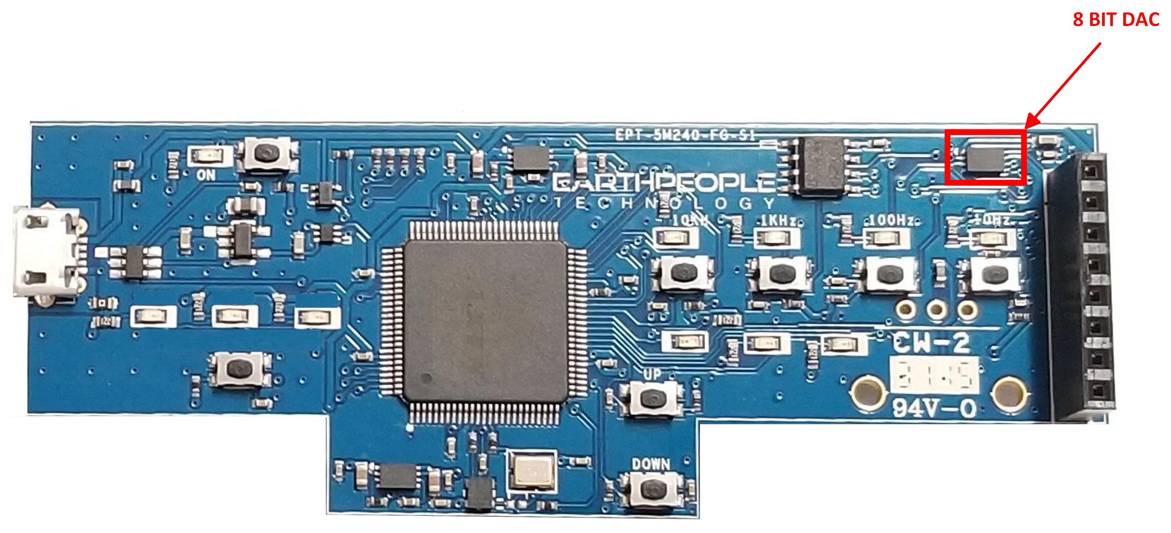
| The BeeProLogic includes a single channel 8 bit DAC. The user can write any 8 bit digital value to the DAC and the associated analog voltage will appear on the output. The DAC is directly connected to the CPLD. The communication path between CPLD and the 8 bit DAC is via SPI bus. |
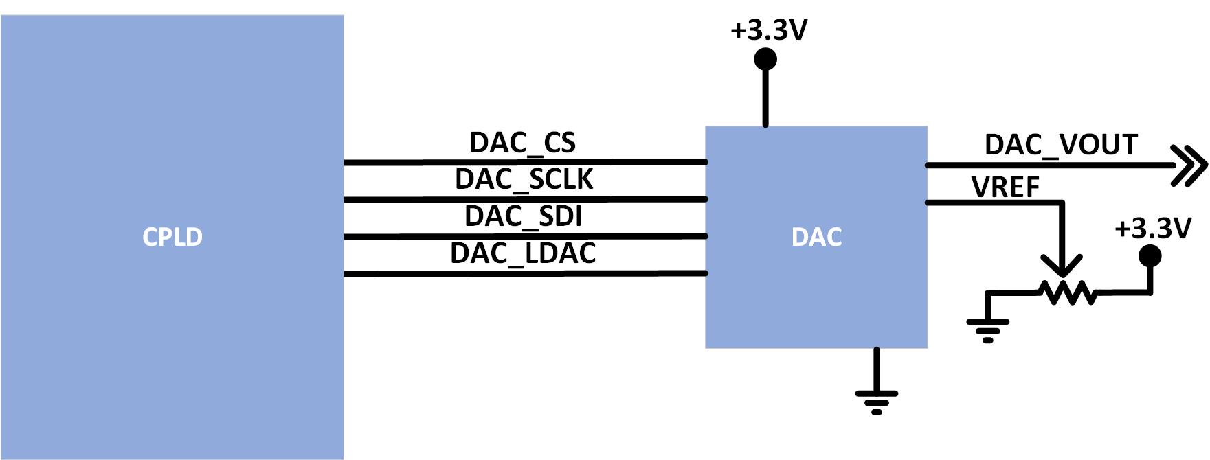
| TThe MCP4901 chip is an SPI Slave. Any SPI host can communicate with the chip at speeds up to 20 MHz. The chip has no minimum SPI clock speed. The chip will respond to any SPI slave at any clock rate as long as it does not exceed 20 MHz. |
User Inputs/Outputs
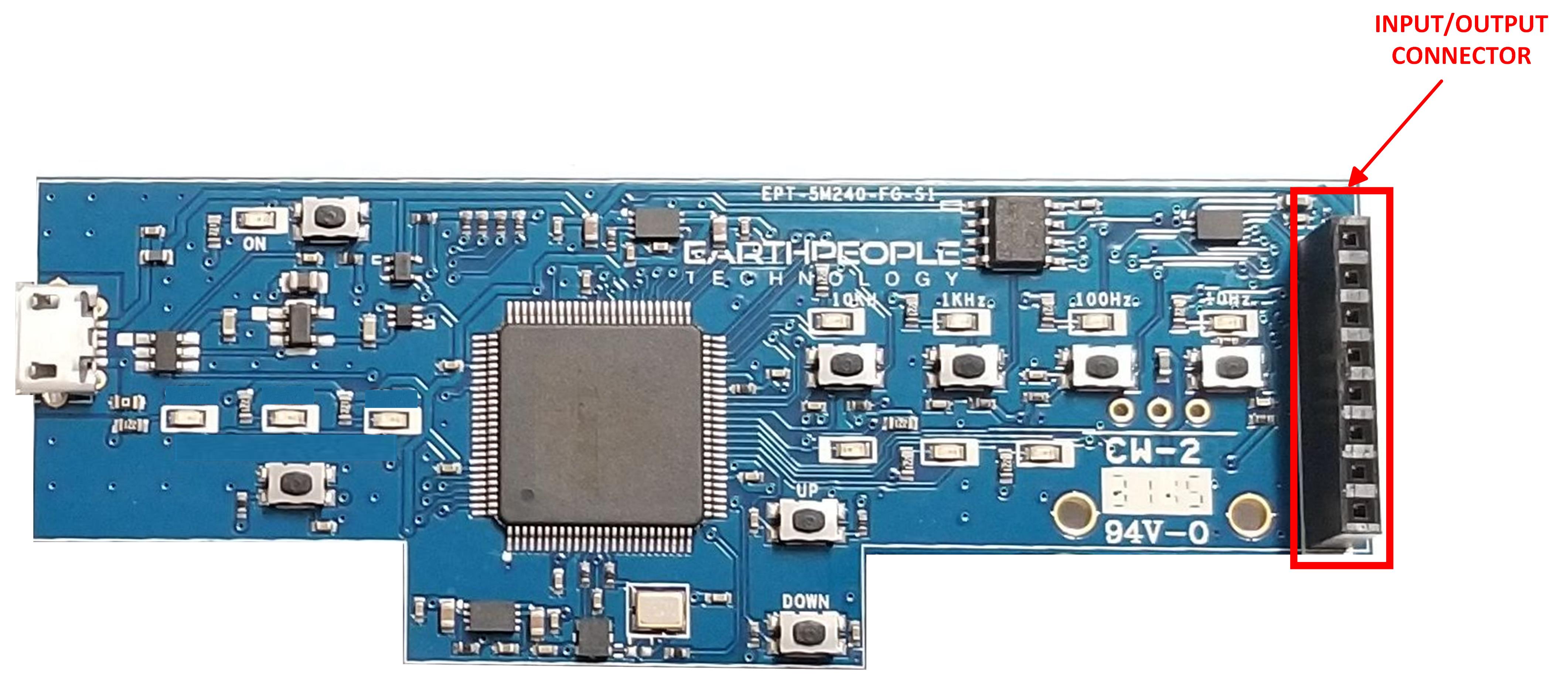
| The BeeProLogic has one 8 pin header that provide 5 digital Inputs and Outputs. All of the I/O’s are +3.3 VDC only. All I/O’s connect directly from the CPLD. The digital pins of the I/O Connector are directly accessible from pins on the CPLD. The user can access these pins by defining them in user HDL code. Then ensure that the pins are connected properly using the Pin Planner tool of Quartus. |
Downloads
| 85-000107 | BeeProLogic CPLD Development System User Manual | BEEPROLOGIC_CPLD_DEV_SYS_UM_V7.pdf |
| 95-000107 | BeeProLogic CPLD Development System Data Sheet | BEEPROLOGIC_CPLD_DEV_SYS_DS_V5.pdf |
| 45-000107 | BeeProLogic CPLD Development System Project DVD | BEEPROLOGIC_CPLD_DEV_SYS_PROJECT_1.0_DVD |
| 55-000107 | BeeProLogic CPLD Development System Schematics | BEEPROLOGIC_SCHEMATICS_V2.pdf |
| 35-000001 | EPT Drivers | EPT_2.08.24.ZIP |
UnoMax Special Purchase

UnoMax Special Purchase
29 Units
Total $724.71
Shipping Included
| The UnoMax makes programmable logic easy with an all inclusive development platform. It includes an Altera 5M570 CPLD, JTAG programmer, and a four channel ADC with 300KS/second sample rate. You can create your HDL code, program it into the CPLD and interact with the hardware via a Windows PC. |
Hardware Features:
|
| The UnoMax DVD provides detailed step by step instructions to quickly guide the user to create a project. The entire Quartus Prime Lite software is included on the DVD. This let’s you bypass the lengthly download process involved in getting the 3.6 GB file. Once the Quartus software is on your desktop, we will show you how to create a project, write you first LED blinky code, compile and program the CPLD. |
|

Programming the CPLD
| The CPLD on the UnoMax can be programmed with the code created by the user. Programming is quick and easy. All that is required is a standard USB cable with a Micro B connector and the Quartus Software installed on the PC. There are no extra parts to buy – just plug in the USB cable and connect the UnoMax to the PC |
![]()

Connecting To Hobby Electronics Made Easy
| The UnoMax easily connects to other Hobby Electronics. The durable 74LVC82245 Bus Transceivers allow up to 50mA per Output on the Stackable Headers. This kind of power can drive all kinds of electronics such as long distance cables, LEDs, and high speed electronics. |
Programmable Logic Code Development
| It also provides a high speed data transfer mechanism between the UnoMax board and a host PC. The UnoMax development system provides a convenient, user-friendly work flow by connecting seamlessly with Altera’s Quartus Prime Lite software. The user will develop the code in the Quartus environment on a Windows Personal Computer. The programmable logic code is loaded into the CPLD using only the Quartus Programmer tool and a standard USB cable. The Active Host SDK provides a highly configurable communications interface between CPLD and host. It connects transparently with the Active Transfer Library in the CPLD code. This Active Host/Active Transfer combination eliminates the complexity of designing a USB communication system. No scheduling USB transfers, USB driver interface or inf file changes are needed. The UnoMax development systemis a unique combination of hardware and software. |
| Use the C# examples included in the DVD to create your own display Window on the PC.The user comes complete with tutorial to instruct the user to easily build a Windows program that can display any data from user code or other electronic device. The C# interface uses similar function calls to the Arduino function calls. |
4 Channel Analog to Digital Converter
| Examine four analog channels running up to 300 KSamples/second. The hardware has been simplified to remove extra cost.The input signals are limited to 0 to +5Volts and the sample rate is shared across all four channels. If you run one channel only, it will take advantage of the 300KSamples/second. If you run four channels, each channel will have a maximum sample rate of 75 KSamples/second. |
Programming Features:
|
Kit Contents
| UnoMax kit contains the UnoMax and a DVD which includes the User Manual that walks the user through setting up the drivers, software, how to use to the test application. There is also a full tutorial in writing yourfirst CPLD project and C# application. All the code for the projects are included. |
Downloads
| 85-000040 | UnoMax CPLD Development System User Manual | UNOMAX_CPLD_DEV_SYS_UM.pdf |
| 95-000040 | UnoMax CPLD Development System Data Sheet | UNOMAX_CPLD_SYS_DS.pdf |
| 45-000040 | UnoMax CPLD Development System Project DVD | UNOMAX_CPLD_SYSTEM_PROJECT_2.7_DVD |
| 55-000040 | UnoMax CPLD Development System Schematics | UNO2_USB_CPLD_SCHEMATICS.PDF |
| 35-000001 | EPT Drivers | EPT_2.08.24.ZIP |
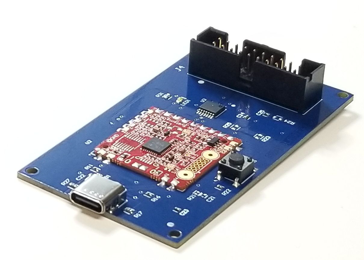
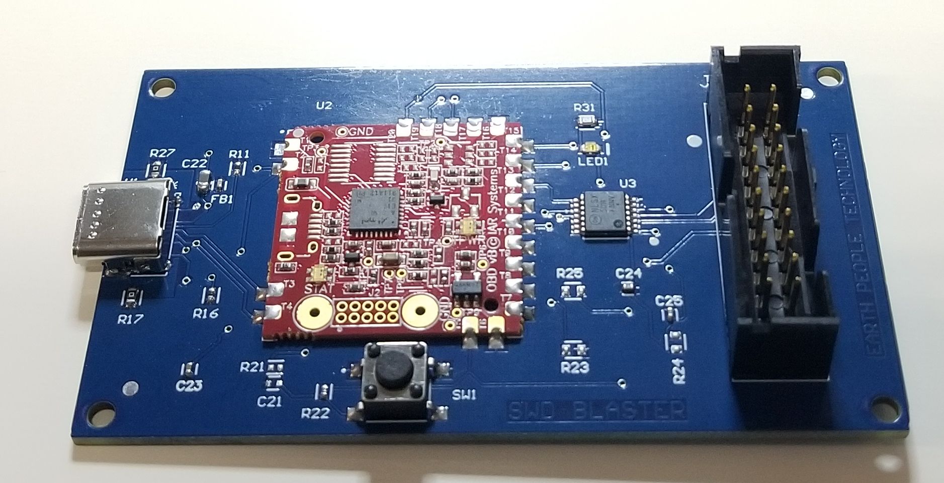
SWD Blaster MCU Programmer

|
SWD BLASTER The SWD Blaster is an easy to use |
| The SWD Blaster is a stand alone programmer for use with IAR Embedded Workbench and capable of debugging most ARM MCU’s. It includes the I-Jet On Board Module from IAR. The SWD Blaster has a maximum speed of 8MHz. I-jet provides a fast debugging platform via JTAG and SWD/SWO with download speeds of up to 1.89 MByte/sec and support for SWO speeds of up to 60MHz. |
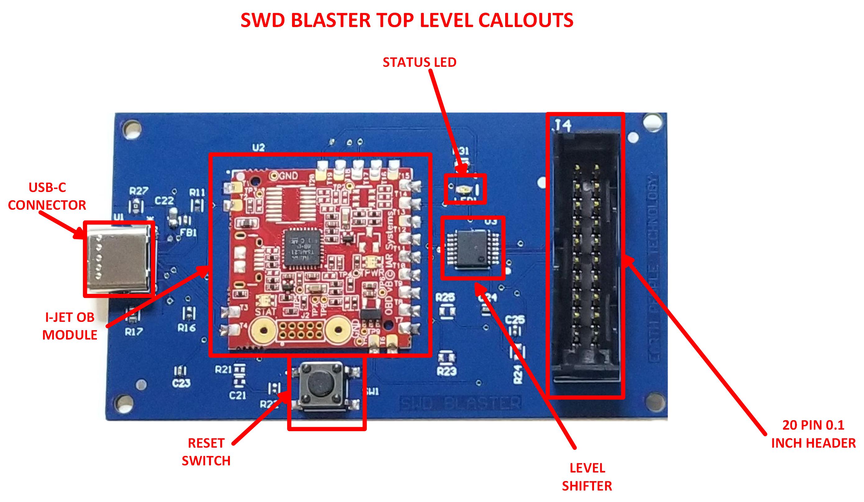
Hardware Features:
|
| The board is powered by USB and connects to target MCU’s via the 20 pin 0.1 Inch header. The SWD Blaster does not require a license. The USB driver for the board is included in the IAR Embedded Workbench software. The board is plug and play and includes a reset pushbutton switch to reset the target. |
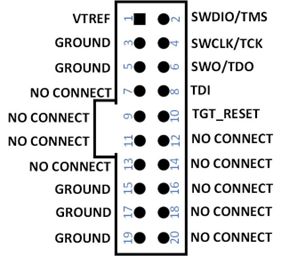
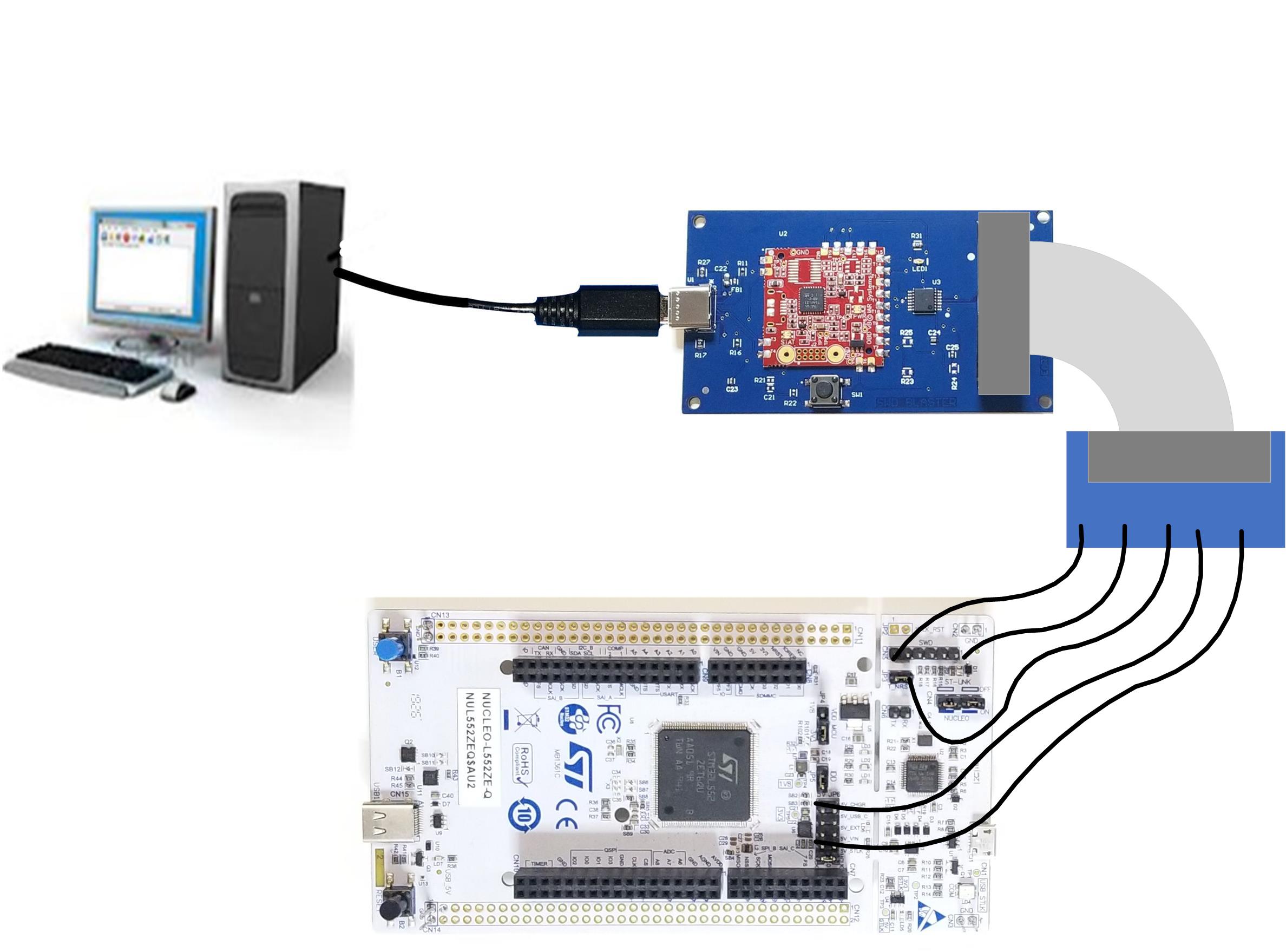
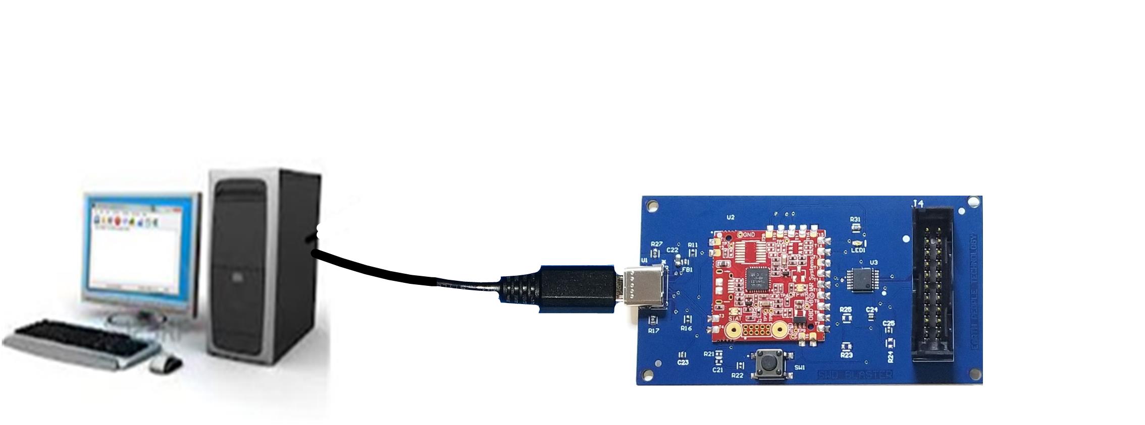
Programming ARM MCUs
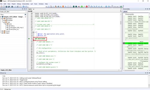
| The SWD Blaster must have the IAR Embedded Workbench installed on the PC. The USB driver is included in the software. Once installed, connect the SWD Blaster using a USB-C cable. Connect the USB cable to a port on the Host PC. Connect the SWD Signals to the target MCU. Use the Embedded Workbench software to connect to the target board. |
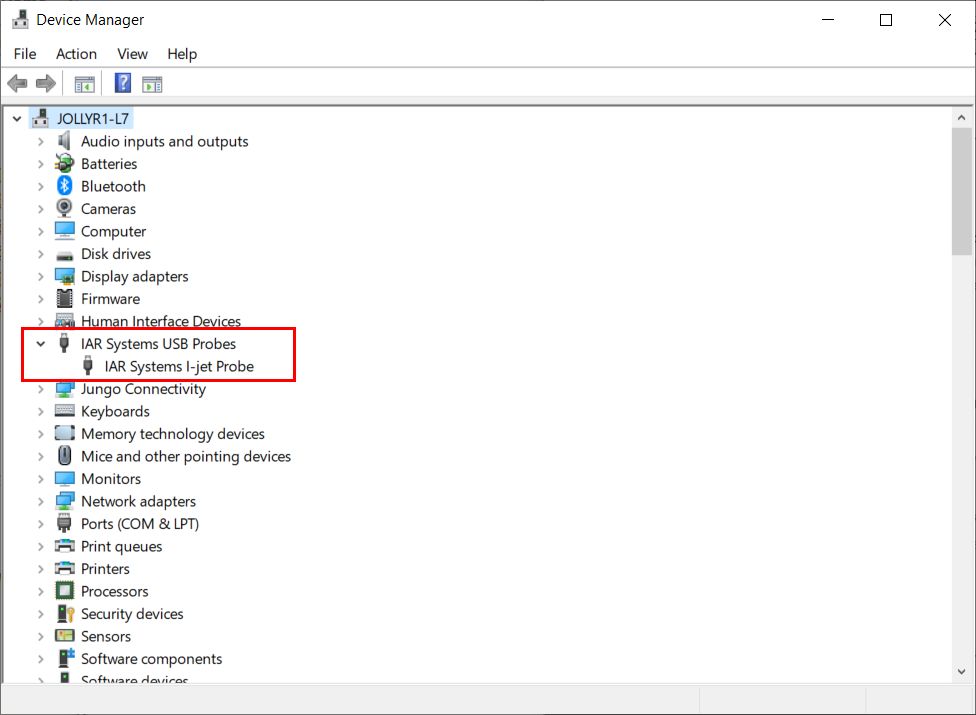
| The SWD Blaster will show up under Device Manager as the I-Jet. When the Embedded Workbench software is open, the user can select I-Jet from the Options Window of the user project. Write user code, compile, download and start debugging. |
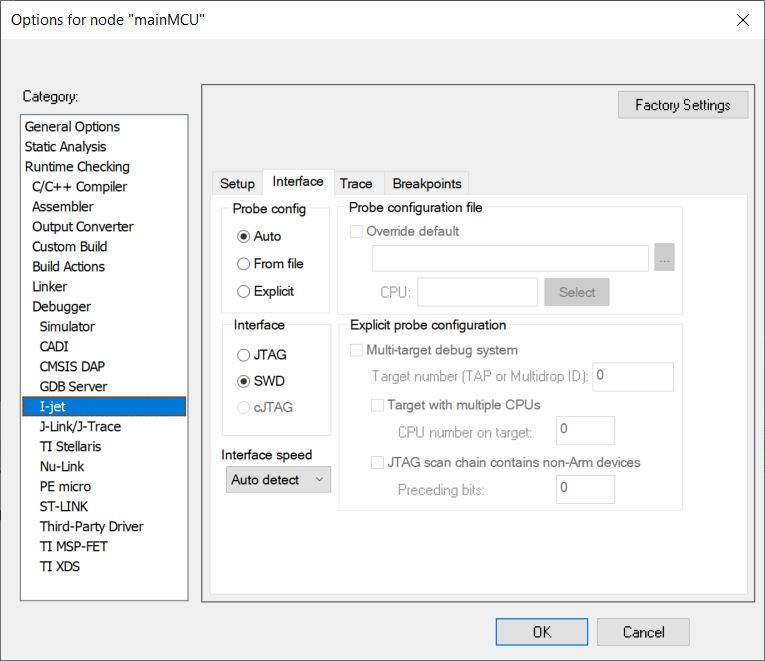
SWD Blaster Functionality
| The SWD Blaster provides the full functionality of the Embedded Workbench software. The user can Download, Debug, Step Go, Pause execution of user code. The OBM provides full SWD JTAG in circuit emulation. The emulation speed is limited to 8MHz. However, this speed is more than adequate for most applications. The OBM provides all of the debugging power of the IAR Embedded Workbench. The user can:
|
Getting Started with Microcontrollers Made Easy
| The SWD Blaster comes with a User Manual that walks the user through getting started with their first Microcontroller (MCU) project development. The User Manual explains how to get the free version of IAR Embedded Workbench and download and install onto the users PC. |
| The User Manual will show to the user how to use Board Support Package such as STM32CubeMX. This software provides a graphical tool that allows configuring the STM32 microcontrollers very easily and generate a complete C project for IAR. STM32CubeMX is free for users. The manual will walk the user through download and install process. Then, it will explain how to set up your first ARM MCU project, GPIO selection, Clock configuration and Peripheral configuration. |
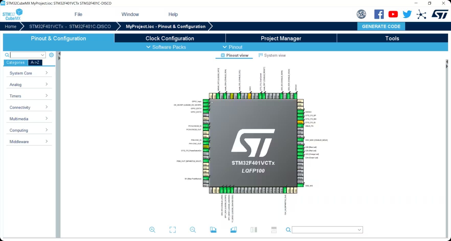
ARM Code Development
| The SWD Blaster User Manual provides an introduction to getting the user set up and working with their first ARM MCU project. After setting up the project using a BSP (Board Support Package), the manual walks the user through how to open a project in IAR EW. The user will make modifications to the default project. The user is instructed to blink an LED attached to a GPIO on the MCU. The manual will explain how to compile the user code, download the code and start the debug process on the target MCU. The User Manual explains the basic features of the debugger environment. It explains the use of breakpoints, watch variables and variable search. The SWD Blaster and User Manuals, Data sheets and example projects will expertly assist getting even the most basic user up and running with their first ARM Code Project. |
Downloads
| 85-001000 | SWD Blaster MCU Programmer User Manual | EPT_SWD_BLASTER_UM_V6.pdf |
| 95-001000 | SWD Blaster MCU Programmer Data Sheet | SWD_BLASTER_DS_V2.pdf |
| 45-001000 | SWD Blaster MCU Programmer Project DVD | SWD_BLASTER_MCU_PROJECT_1.0_DVD |
| 55-001000 | SWD Blaster MCU Programmer Schematics | EPT_IOBM_PT_W2_V1.SCHEMATIC.PDF |
| 35-001000 | SWD Blaster Drivers | CDM212364_Setup.ZIP |
DSO 100M Development Board
The DSO 100M is a Complete Open
Source Digital Storage Oscilloscope
Development System. It Includes
Four Channels of Analog Input With
a Dedicated 80 MHz Sampling Rate
per Channel
| The Earth People Technology DSO 100M development system is a fully functional USB Digital Storage Oscilloscope. It was designed to be open, flexible and easy to modify. This Open Source Development System allows the user to understand the basics of the typical DSO. All source code along with compiled projects are made available. The user can modify the Verilog code in the FPGA as well as the C# project known as the UnoProlyzer. |
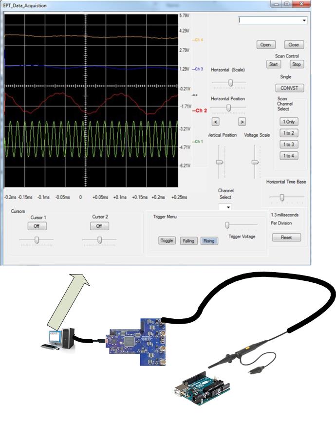
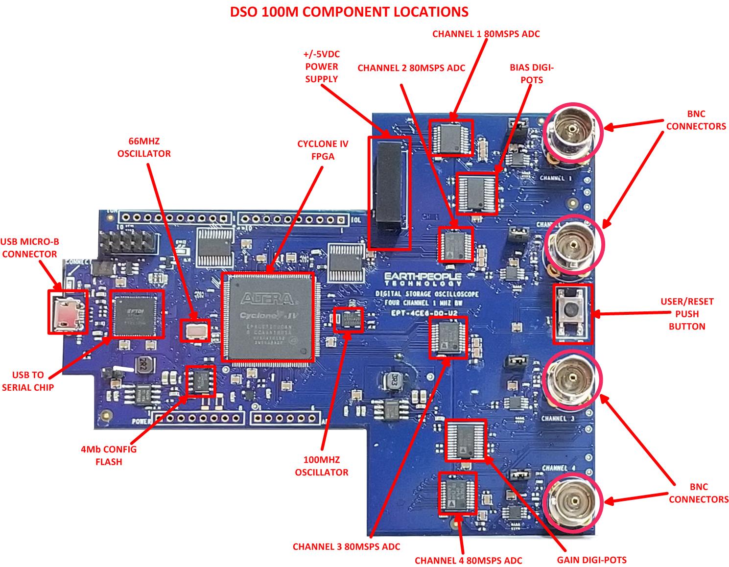
| The DSO 100M includes all the hardware necessary to understand the modern Digital Storage Oscilloscope. Each section of the hardware has been meticulously designed to ensure consistent operation with the PC application. Block Diagram below |
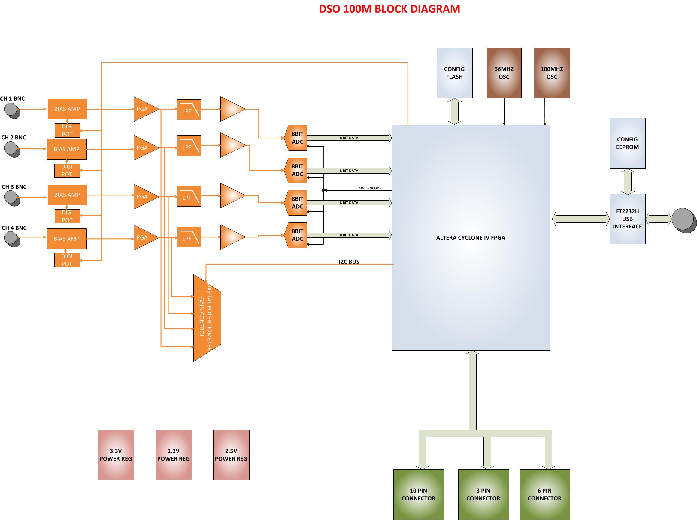
Hardware Features:
|
| The DSO 100M analog front end has been meticulously designed and tested to provide a noise and distortion free analog path to the ADC. To ensure the distortion free signal, a bias amplifier is included using an OPA1602 Op-Amp along with digital selectable gain using a AD5263 Digital Potentiometer. Each BNC connector is 50 Ohm impedance matched on the PCB. A precision +/- 5V DC-DC brick power supply is used to keep the power matched used in powering the Op-Amps and Digital Potentiometers. |
Kit Contents:
|
DVD Contents:
|
Verilog Code Description:
| The FPGA project is written in Verilog code. The code uses EndTerms to allow a flexible communications between the PC application and the FPGA. All communications go through the UC_Controller block. This module interfaces to a memory block and a control register block. When the PC application needs to perform an action, it will write the data to the memory block. Then, it will write an action bit to one of the control registers. The control registers are monitored in the Top Level code to initiate the action. |
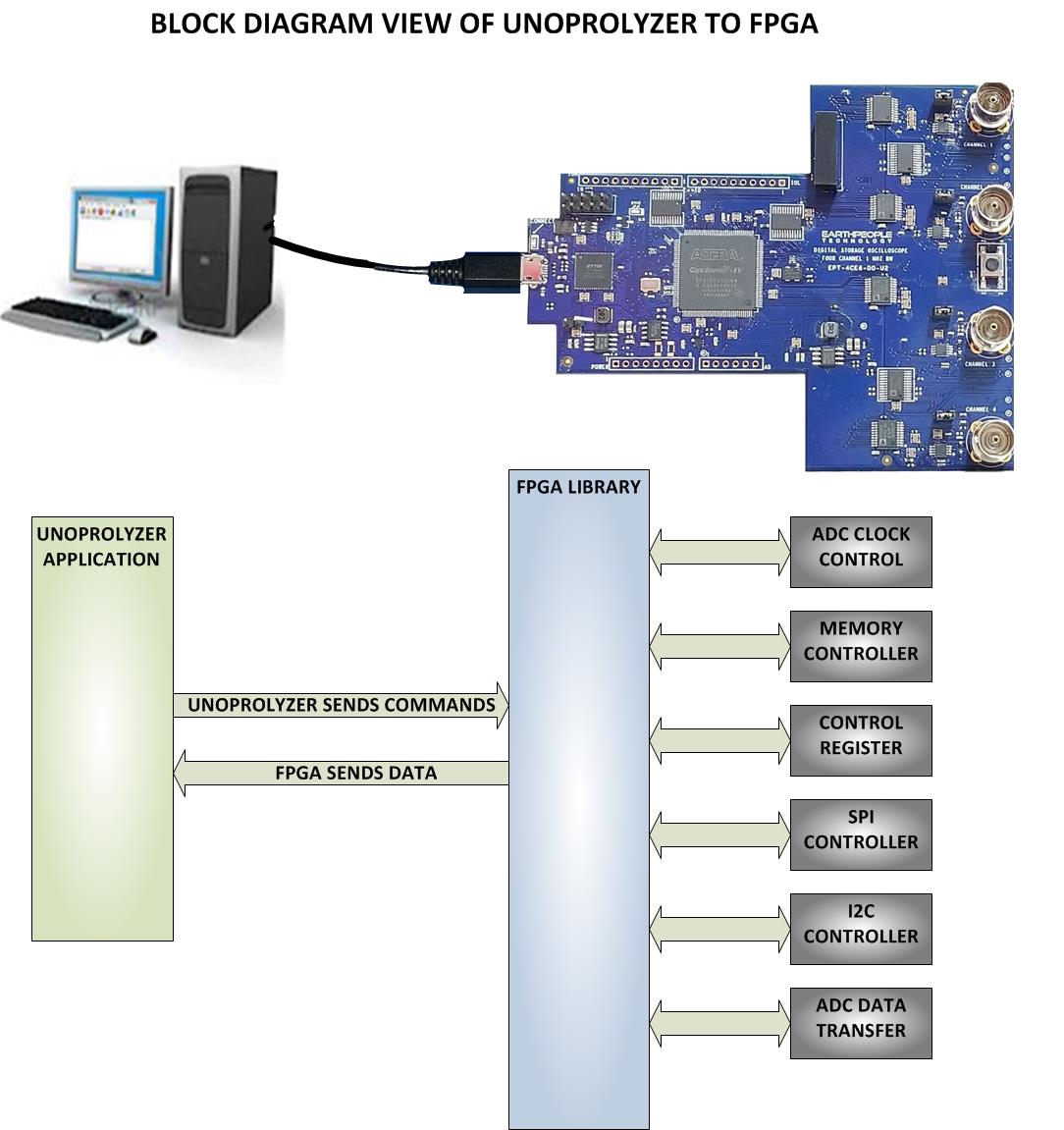
| There are three main components that comprise the communication part of the FPGA code base. There are also several sub-processes that are required for the proper operation of the entire DSO 100M. The communication components: |
- Host Interface Component
- ADC Sample Storage Component
- Data Transmit Component
These components depend on the Active Transfer Library
(and conversely on the Active Host dll) to communicate,
initiate functions, start ADC sampling and transmit data.
All source files, compiled projects, testbenches, test
models are included on the EPT Project DVD. Locate the
Projects_HDL folder on the DVD for the project.
The following components make up the FPGA Code Base:
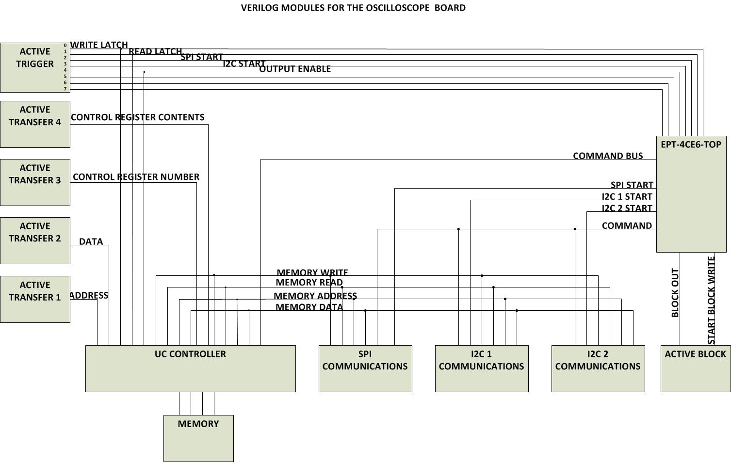
| The entire FPGA project has been simulated and includes and advanced testbench. The user manual includes an extensive description of the Verilog Modules and the interconnection between them. The testbenches and models have been written without any vendor specific IP, so the user can easily set up the free Modelsim from Intel/Altera and get simulating quickly. |

Software Description:
| The DSO 100M utilizes the UnoProLyzer application to control and display the oscilloscope results on a Windows PC. The UnoProLyzer is a C# Windows application. This means it is an event driven application. Any event such as a button press or timer expiring will initiate a function in the application. The application communicates with the FPGA Code via EndTerms. It sets up the buttons, timers and display in the Window. The applications waits in idle for the user to initiate an event, or an automatic event initiation. |
User events are as follows:
- Load the application
- Connect to the DSO 100M board
- Select channels to display
- Start the oscilloscope
- Select channel to process
- Horizontal Zoom on selected channel
- Vertical dynamic range selection
- Horizontal Timebase selection
- Triggering
- Cursor Measurement
Automatic Events are:
- Countdown Timer Expiration
- ADC storage data callback
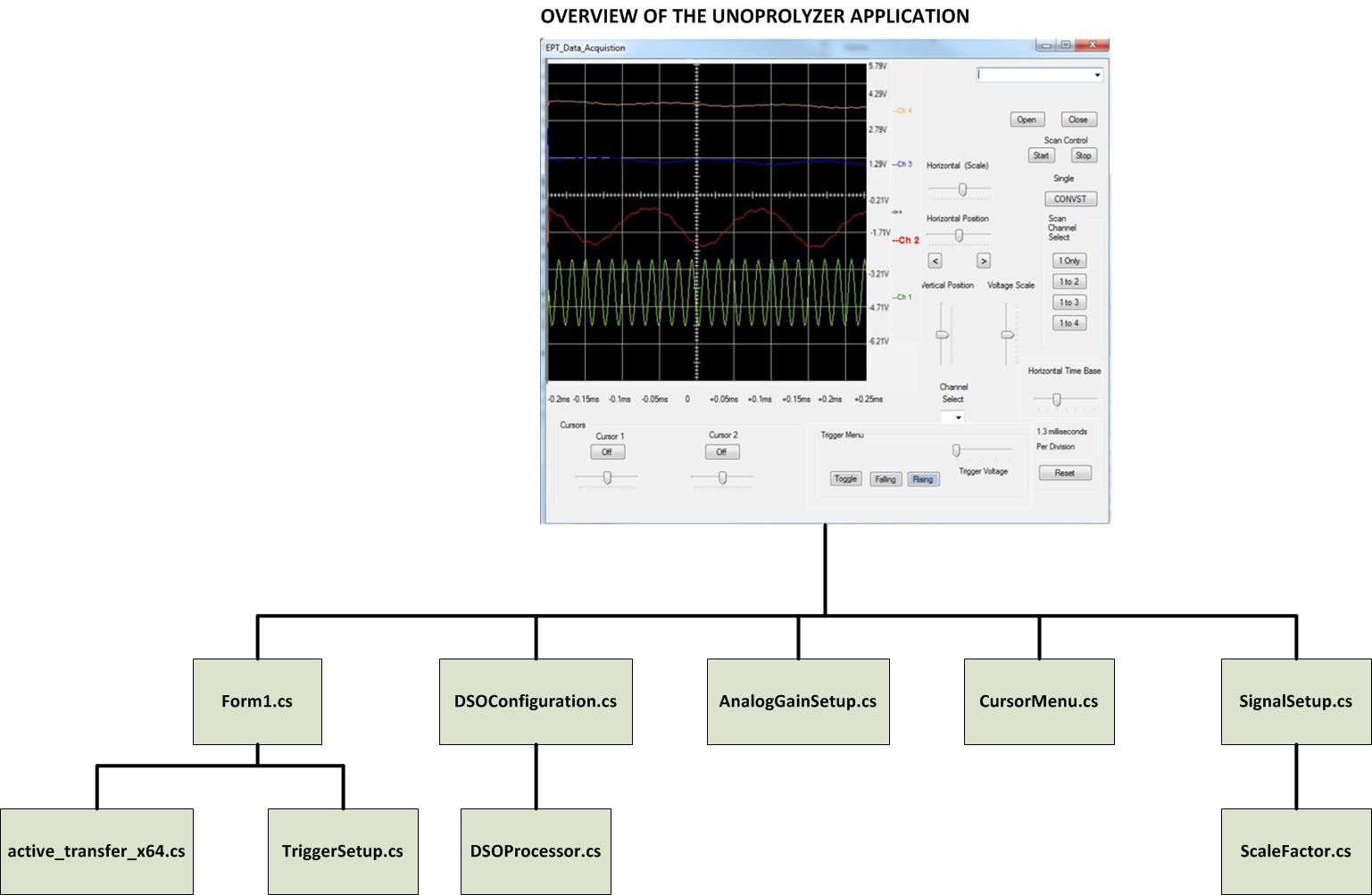
Software Flow Diagram:
| The software flow diagram below shows some of the complexity of the UnoProLyzer. Each path starts off with an event, either user or automatic. The user will select channels to display, set the Horizontal Timebase to use by the ADC’s, set the Vertical Dynamic Range to display of each channel, then start the display of the analog signals acquired by each ADC. |
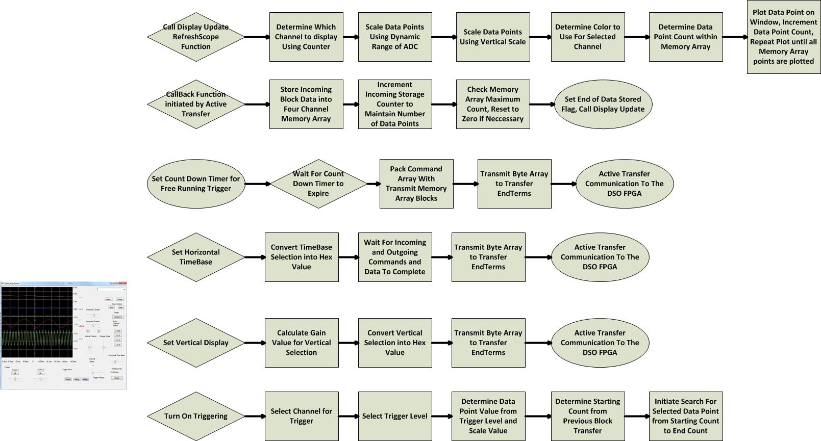
DSO Programming:
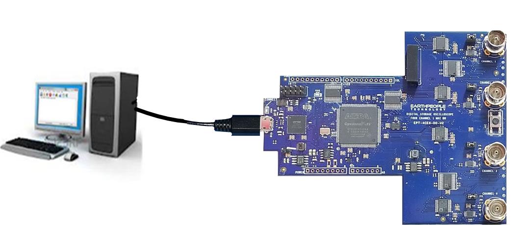
| The DSO is easily programmed from the Quartus Lite Software. Just plug a Micro B USB cable from an open Port on the PC to the Connector on the DSO 100M and load the drivers. A proprietary *.dll from EPT allows the DSO 100M Configuration Flash to be programmed directly from Quartus. |
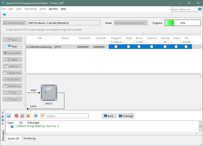
Downloads
| 85-000100 | DSO 100M Development System User Manual | EPT_DSO_100M_DEV_SYS_UM_V45.pdf |
| 95-000100 | DSO 100M Development System Data Sheet | EPT_DSO_100M_DEV_SYS_DS_V42.pdf |
| 45-000100 | DSO 100M Development System Project DVD | DSO_100M_DEV_SYS_PROJECT_4.0_DVD |
| 55-000100 | DSO 100M Development System Schematics | EPT_4CE6_DO_U2_SCHEMATIC_V4.PDF |
| 35-000001 | EPT Drivers | EPT_2.12.36.ZIP |
| 05-000001 | Older Version DVD | DSO_100M_DEV_SYS_PROJECT_2.8_DVD.zip |
Seven Segment LED Board
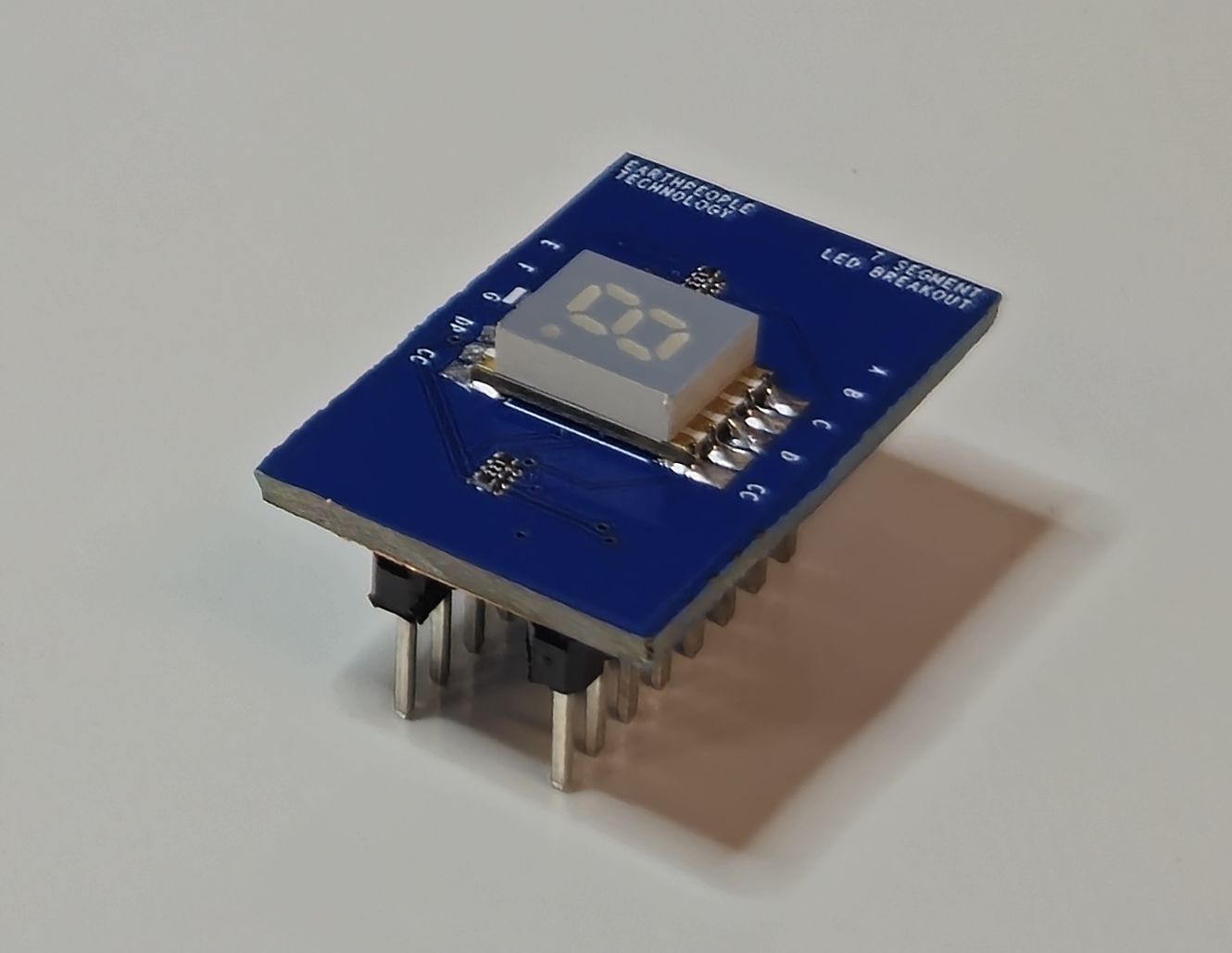
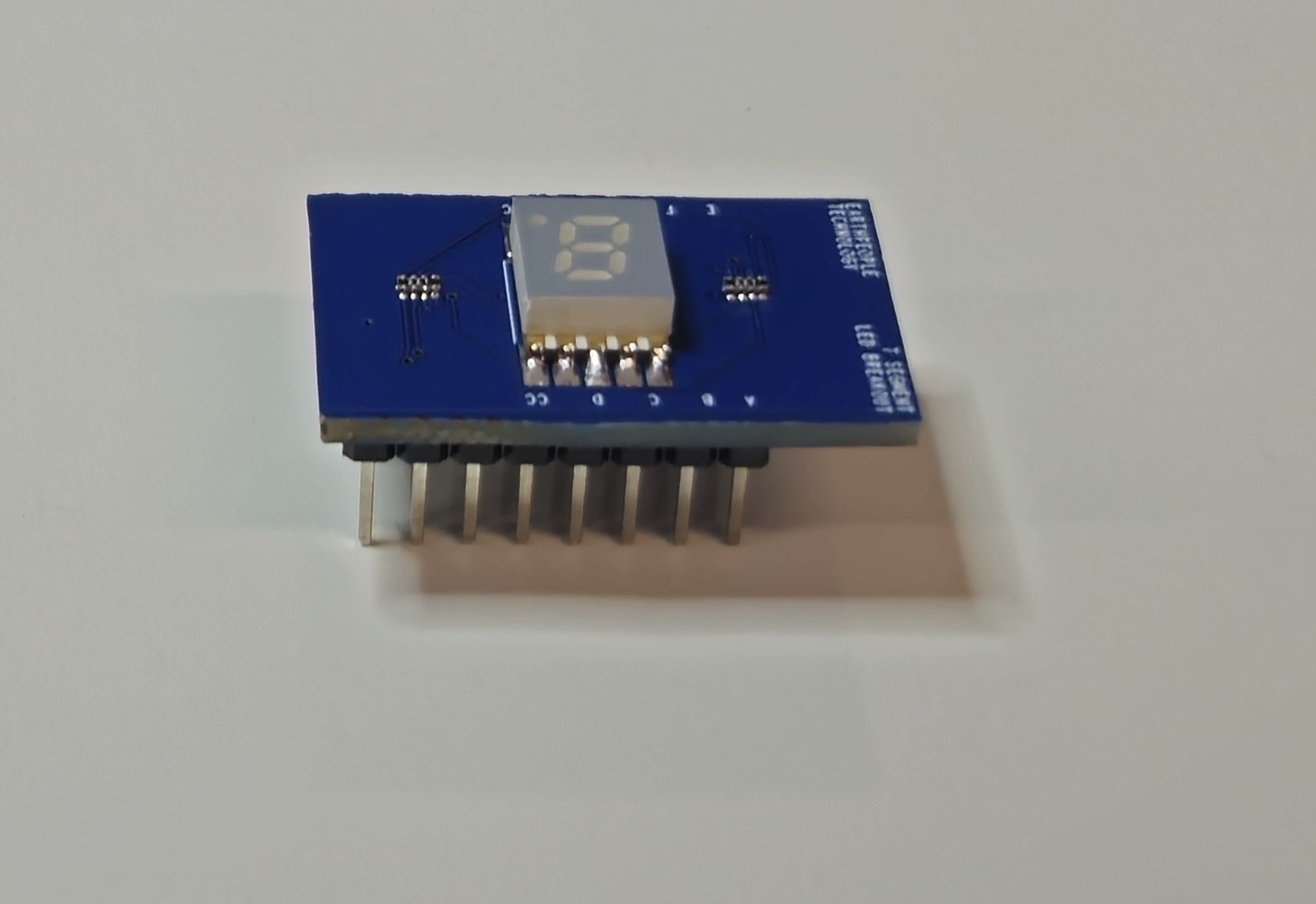 Seven Segment LED Board
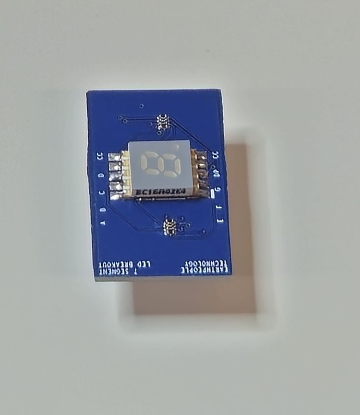
Seven Segment LED BoardThe EPT-ACSA02-LD-X2 is a breakout board that includes one Seven Segment LED. |
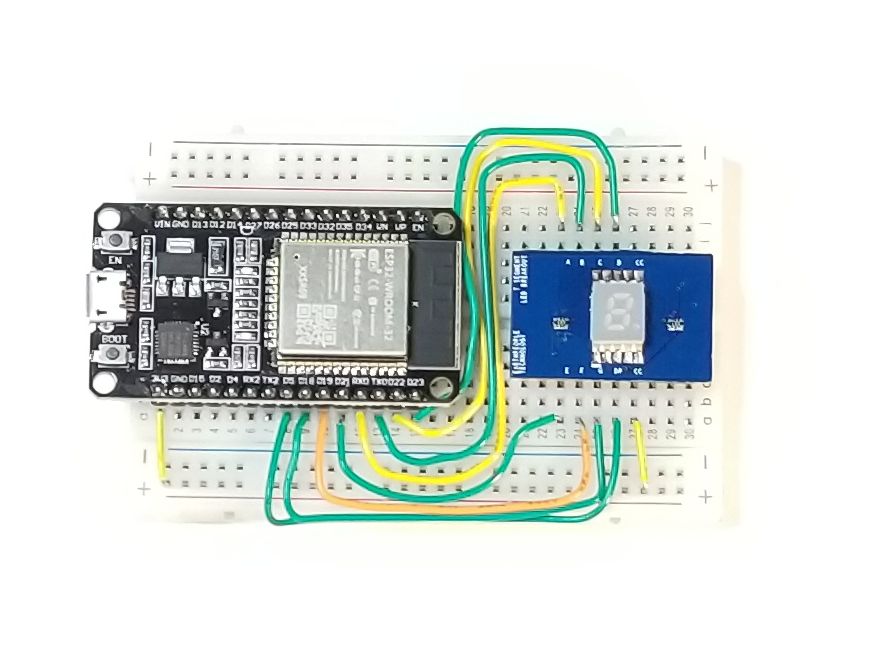
| The Seven Segment LED board uses one ACSA02-41SGWA-F01 manufactured by Kingbright. The Display is 0.2 inch digit height. It has low current operation and excellent character appearance. The Super Bright Green source color devices are made with Gallium Phosphide Green Light Emitting Diode. |
Hardware Features:
|
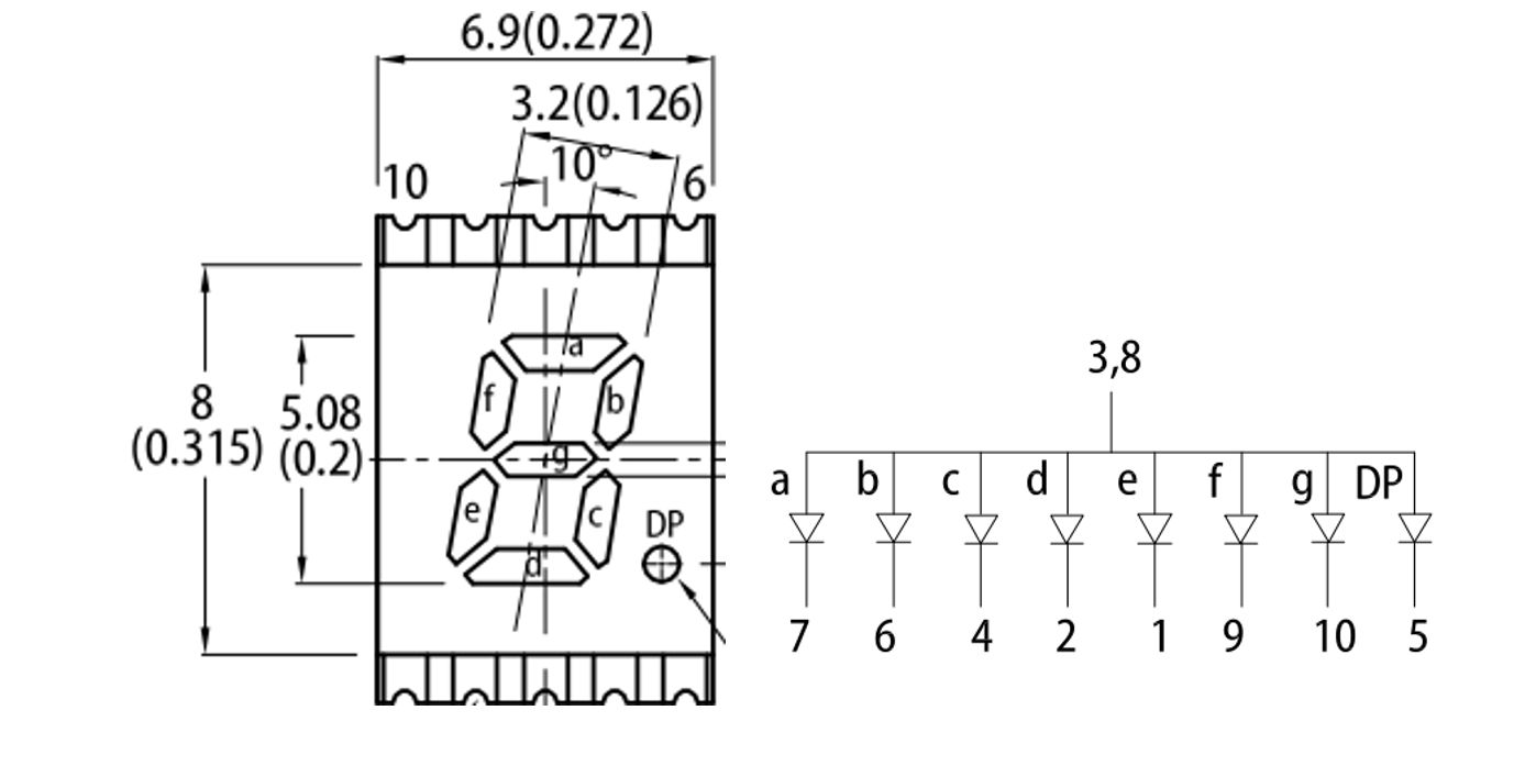
Description
| Each LED current limiting resistor is calculated to provide 5mA in each of the LED Segments. These current limiting resistors cannot be changed The ACSA02-41SGWA-F01 chip is a current sink and can be connected to any MCU. The anode should be connected to +3.3V. The reason for this is the Series resistors are calculated for current limiting based on +3.3V. Changing the anode voltage to another source will change the brightness emitting from each LED. Because the ACSA02-41SGWA-F01 chips are current sink, the user can connect to either +5V or +3.3V Arduino (or other MCUs) and control each LED. |
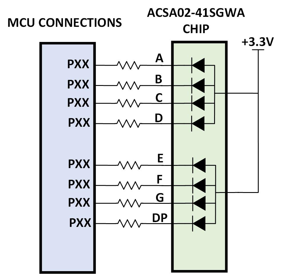
LED Electrical SpecificationsEach LED current limiting resistor is calculated to provide 5mA in each |
| Parameter | Symbol | Emitting Color | Value | Units |
|---|---|---|---|---|
| Peak Wavelength | Super Bright Green | 565 | nm | |
| Dominant Wavelength IF = 10mA | Super Bright Green | 568 | nm | |
| Spectral Bandwidth at 50% | Super Bright Green | 30 | nm | |
| Forward Voltage IF = 10mA | Super Bright Green | 2.0 | V | |
| Reverse Current (VR = 5V) | Super Bright Green | 10 | uA |
Easily Control Seven Segment LED Display from an Arduino
| The Seven Segment LED Board comes with example software that blinks individual LEDs from the External MCU (Such as the Arduino Mini Pro). The user can display characters using each LED Display. The MCU will provide pulse width modulated control for each LED. Changing the duty cycle of each LED changes the overall brightness of each segment of the LED Display. |
Downloads
| 85-000040 | Seven Segment LED Board User Manual | LED_SEVEN_SEGMENT_BOARD_UM_V1.pdf |
| 95-000040 | Seven Segment LED Board DataSheet | LED_SEVEN_SEGMENT_BOARD_DS_V2.pdf |
| 45-000040 | Seven Segment LED BoardProjects DVD | SEVEN_SEGMENT_LED_PROJECT_1.0_DVD.ZIP |
| 55-000040 | Seven Segment LED Board Schematics | LED_SEVEN_SEGMENT_SCHEMATIC_V1.pdf |
ESP32 WROOM DEVELOPMENT BOARD
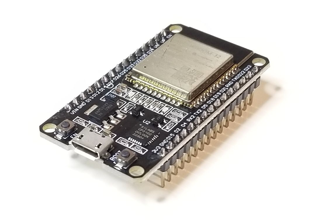
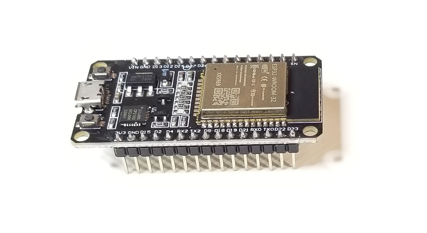
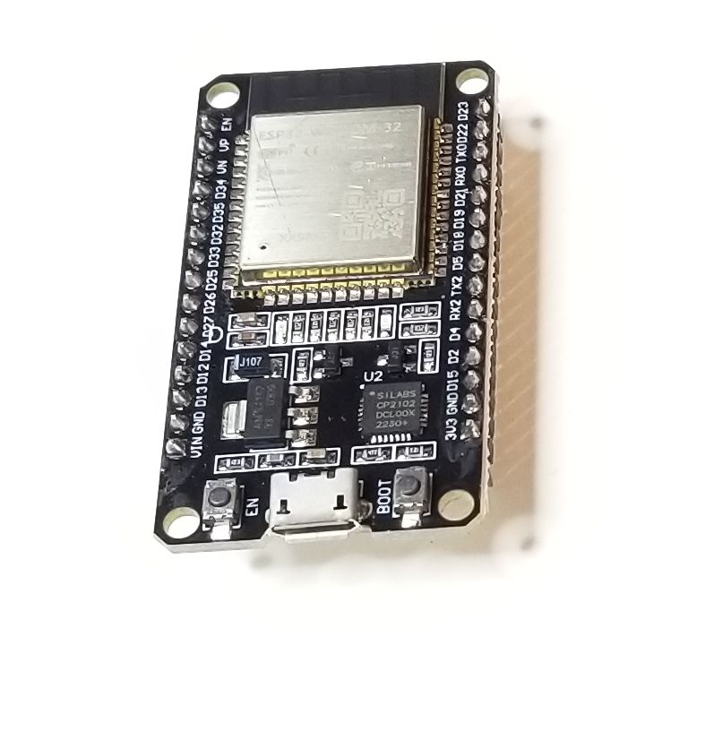
|
ESP32 WROOM The ESP32 is an easy to use |
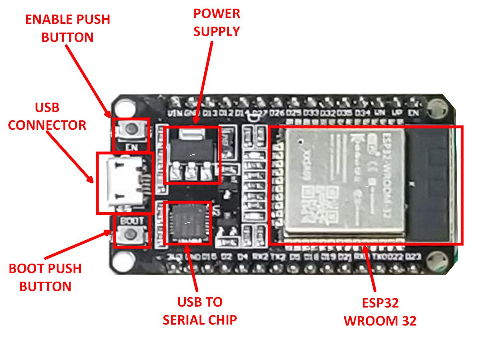
| The ESP32 Development Board is a board created around ESP32 WROOM 32 chip containing voltage regulator and USB programmer circuit for ESP32 chip, and a few many other features. For application development there is a choice between Arduino IDE or ESP-IDF (Native platform). Mostly users choose the Arduino IDE because of its simplicity and compatibility. ESP32 Development Board comes with a pre-installed firmware which allows to work with the interpreted language, sending commands through the serial port (CP2102 USB to Serial chip). The ESP32 Development board is specially designed to work on breadboard. It has a voltage regulator that allows it to feed directly from the USB port. The input/output pins work at 3.3V. The CP2102 chip is responsible for USB to serial communication. |
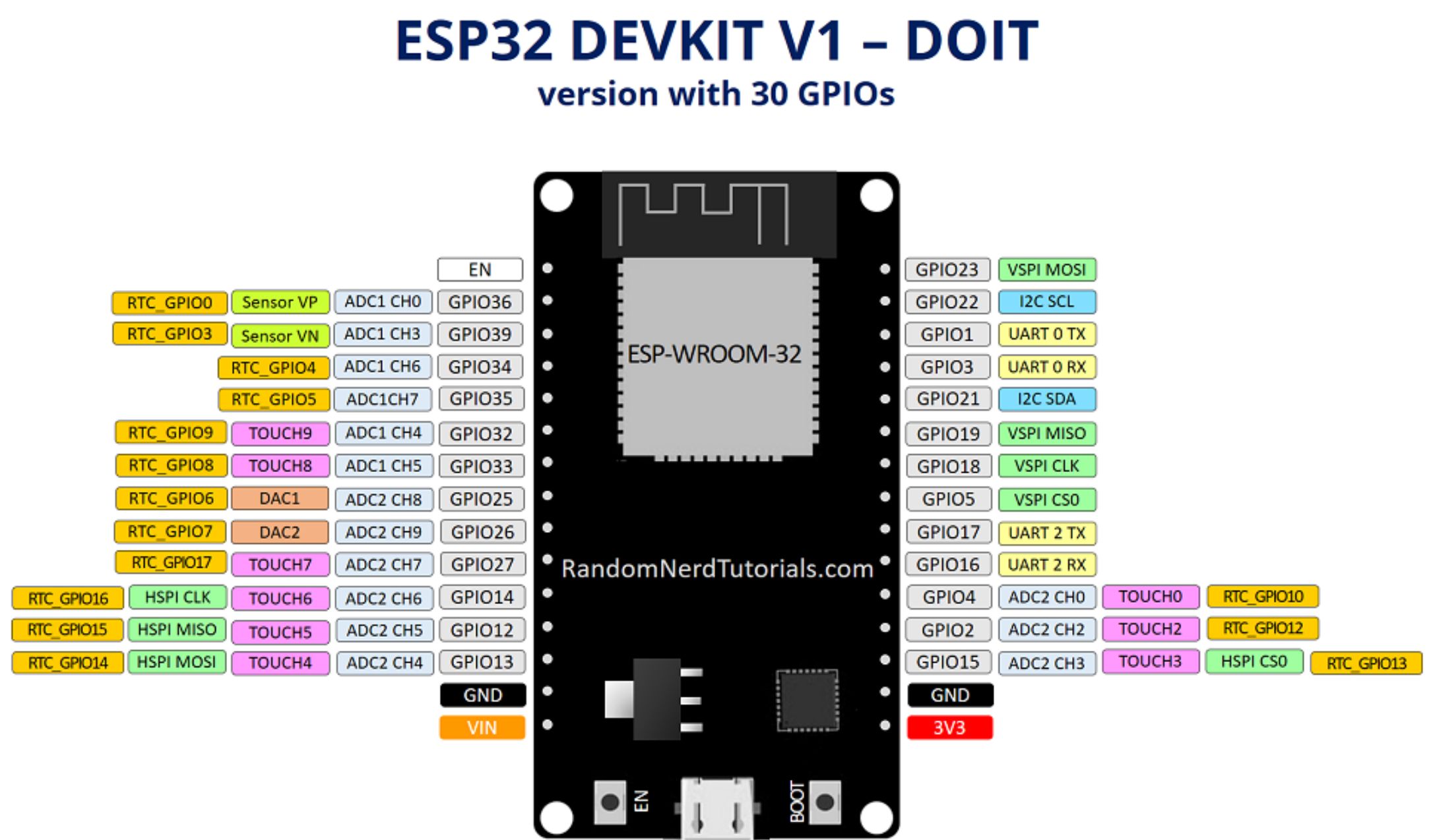
Hardware Features:
|
MCU + Wifi + BLE
| The board functions as a 32 MCU and provides all peripherals expected from an MCU. It also includes a Wifi transceiver unit and a BLE 4.2 Radio. All of this functionality is easily accessed through the Arduino IDE. An easy to use, intuitive software interface to build your software programs such as Weather Station, Indoor Asset Tracking, Robotics and much more. |
Programming The ESP32 MCUs
| Programming the ESP32 with User Software is easy using the Arduino IDE. The ESP32 WROOM Development board includes a USB to Serial chip. Just connect the board to an open USB Port on your PC using a Micro-B cable. Then open the Arduino IDE software, select the board from the library. Write your software, then hit the “Upload” button. It’s as easy as that. |
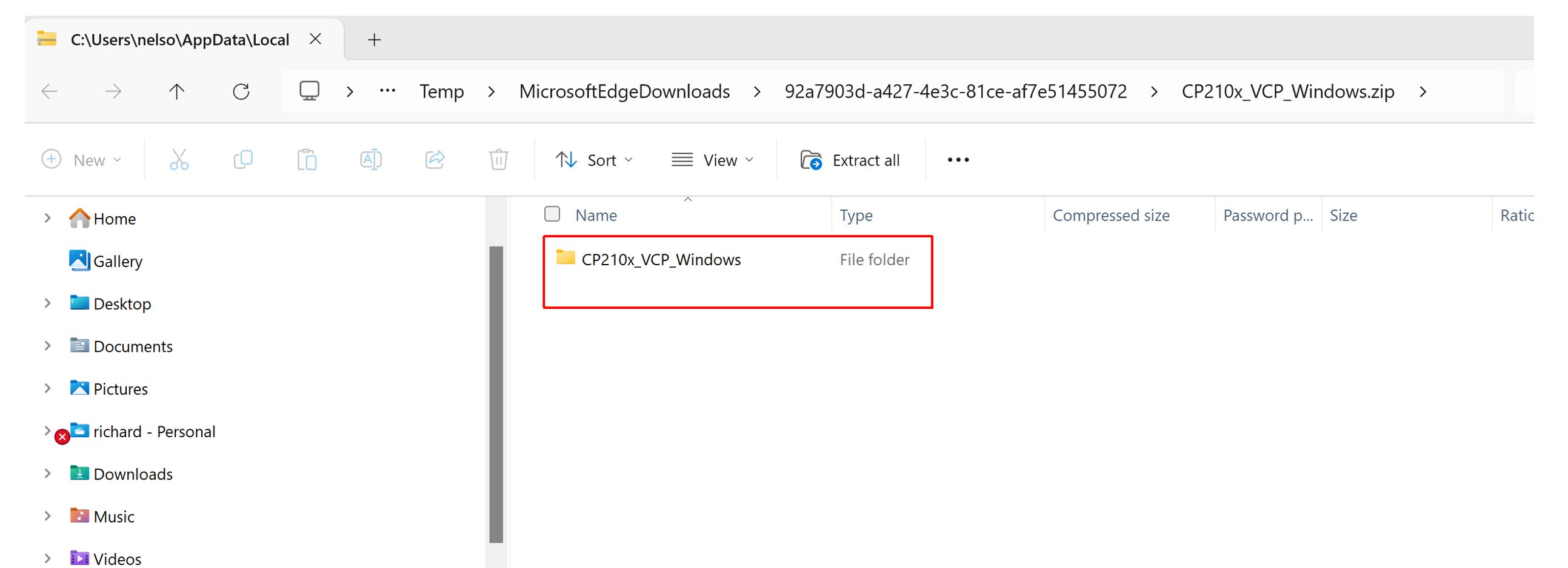
| When the ESP WROOM Development Board is connected to an open USB Port the USB driver for the CP2109 chip is loaded. You will be able to see this chip under “Device Manager” as a COM Port. Once the ESP32 board appears as a COM Port, the Arduino IDE will be able to connect to it. |
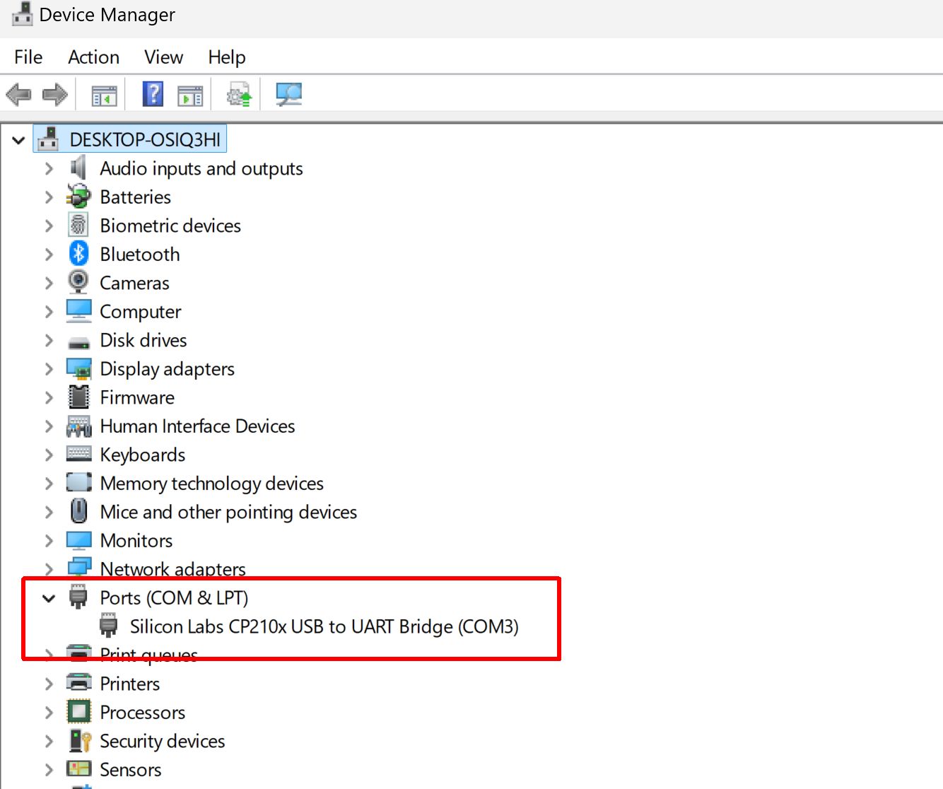
Connecting the Arduino IDE to ESP32
| Once the ESP32 board is connected and the driver is loaded, Open the Arduino IDE, then click on the “Boards Manager” button and search the left side of the Window for the ESP32 Libraries. Click on “Install” and the software will automatically install all the available libraries for several ESP32 Development boards. |
| Once all the ESP32 libraries are installed, you can go Tools->Board and select the “ESP32 Dev Module”. Then go to Tools->Port and select the COM Port that the ESP32 WROOM Development board is attached to. With these items selected, you can now write and execute your own code. |
| The User Manual will show to the user how select one of the pre-compiled sample programs and load it, compile it and upload it to the ESP32 MCU. The User Manual will show the user how to build the projects using a bread board, ESP32 WROOM Development Board, Wire Kit and Device (Such as LED RGB. Breakout Board or Seven Segment LED Display Board). |
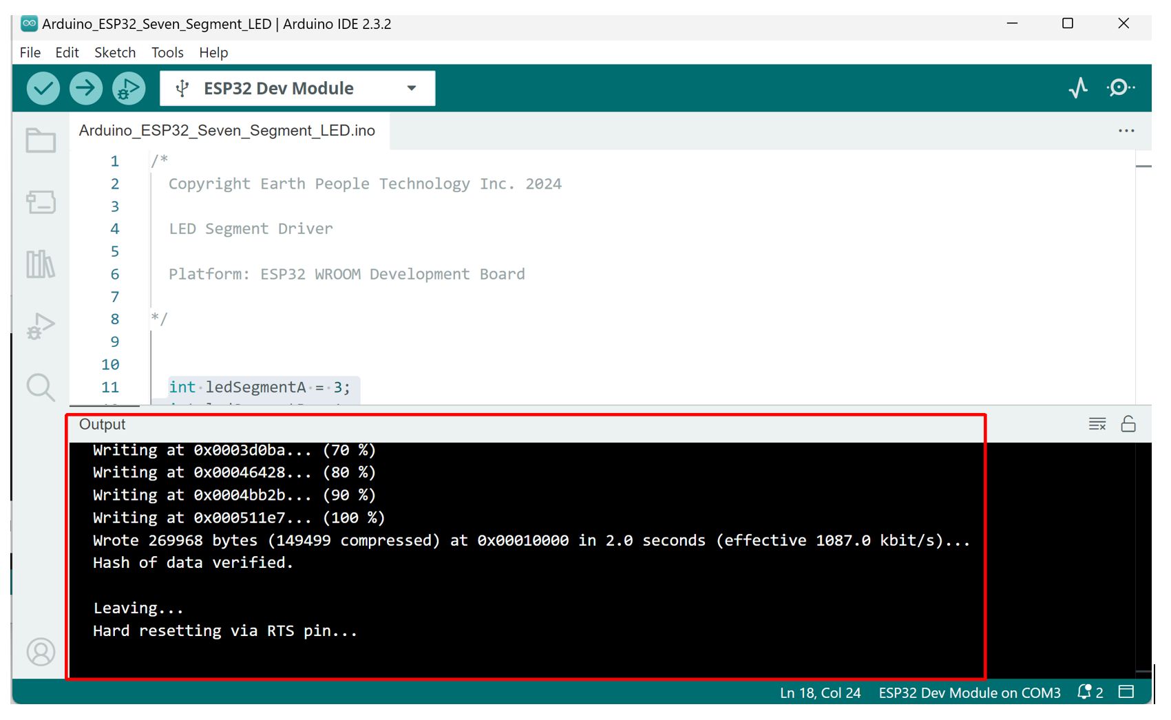
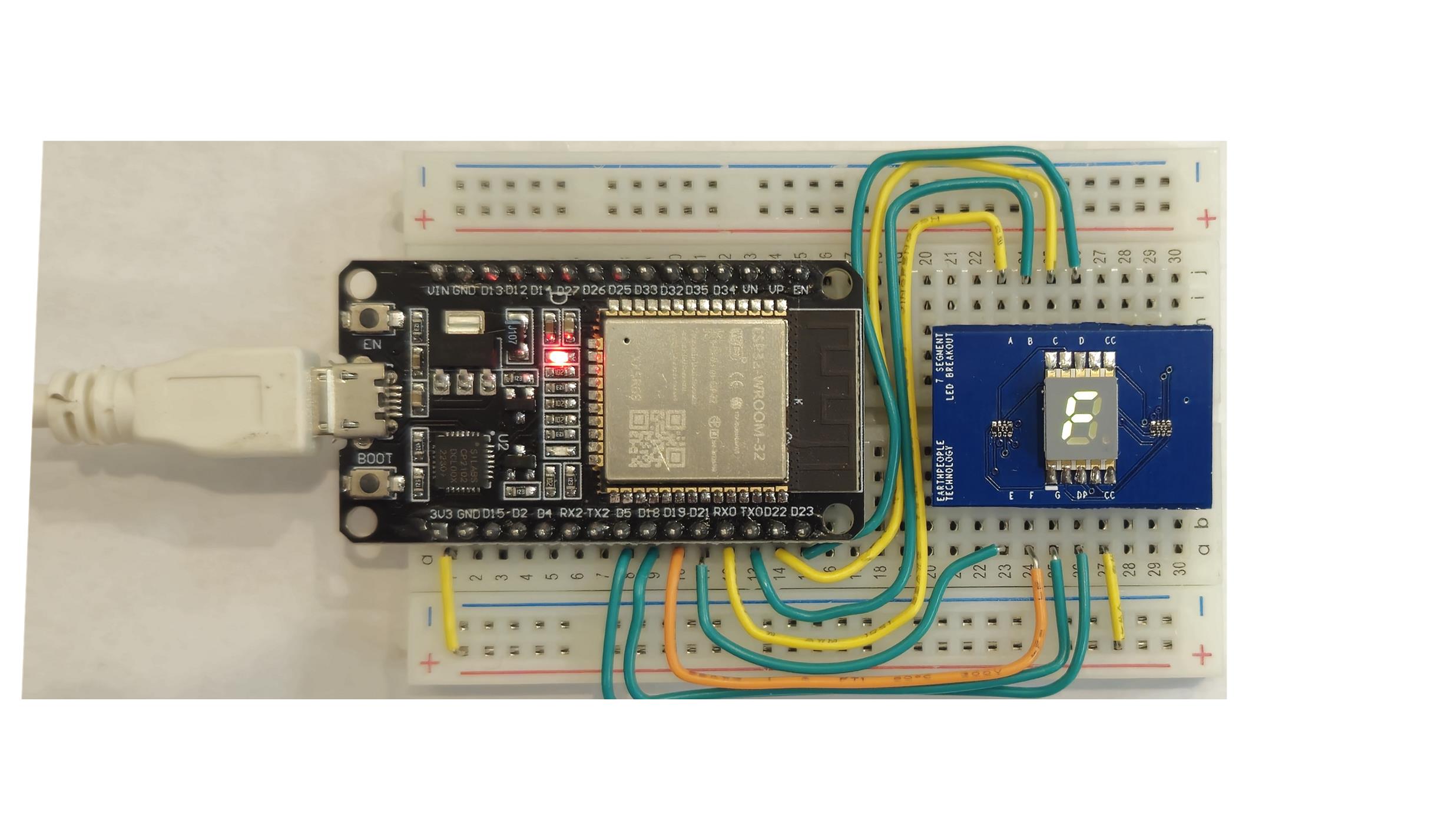
ESP32 Code Development
| With your first programmed loaded and working on to the ESP32 WROOM Development Board completed, you can start on more advanced projects. More advanced projects will include getting started with WiFi. There are several pre-compiled WiFi projects under the Arduino ESP32 Examples. These examples are easy to use. Just open the sketch, upload and start examining the results. The ESP32 WROOM Development Board is a complete Development Kit that is easy to get started, easy to develop code and easy to get advanced projects perfected. This kit is great for beginners, great for intermediate programmers, and great for advanced projects. |
Downloads
| 85-001020 | ESP32 WROOM Development Board User Manual | ESP32_WROOM_DEV_BOARD_UM_V3.pdf |
| 95-001020 | ESP32 WROOM Development Board Data Sheet | ESP32_WROOM_DEV_BOARD_DS_V2.pdf |
| 45-001020 | ESP32 WROOM Development Board Project DVD | ESP32_DJ_SNACK_PACK_PROJECT_4.0_DVD |
| 55-001020 | ESP32 WROOM Development Board Schematics | ESP32-Core-Board-V2_sch.PDF |
| 35-001020 | ESP32 WROOM Development Board Drivers | CP210x_VCP_Windows.ZIP |
CycloFlex FPGA Development Board
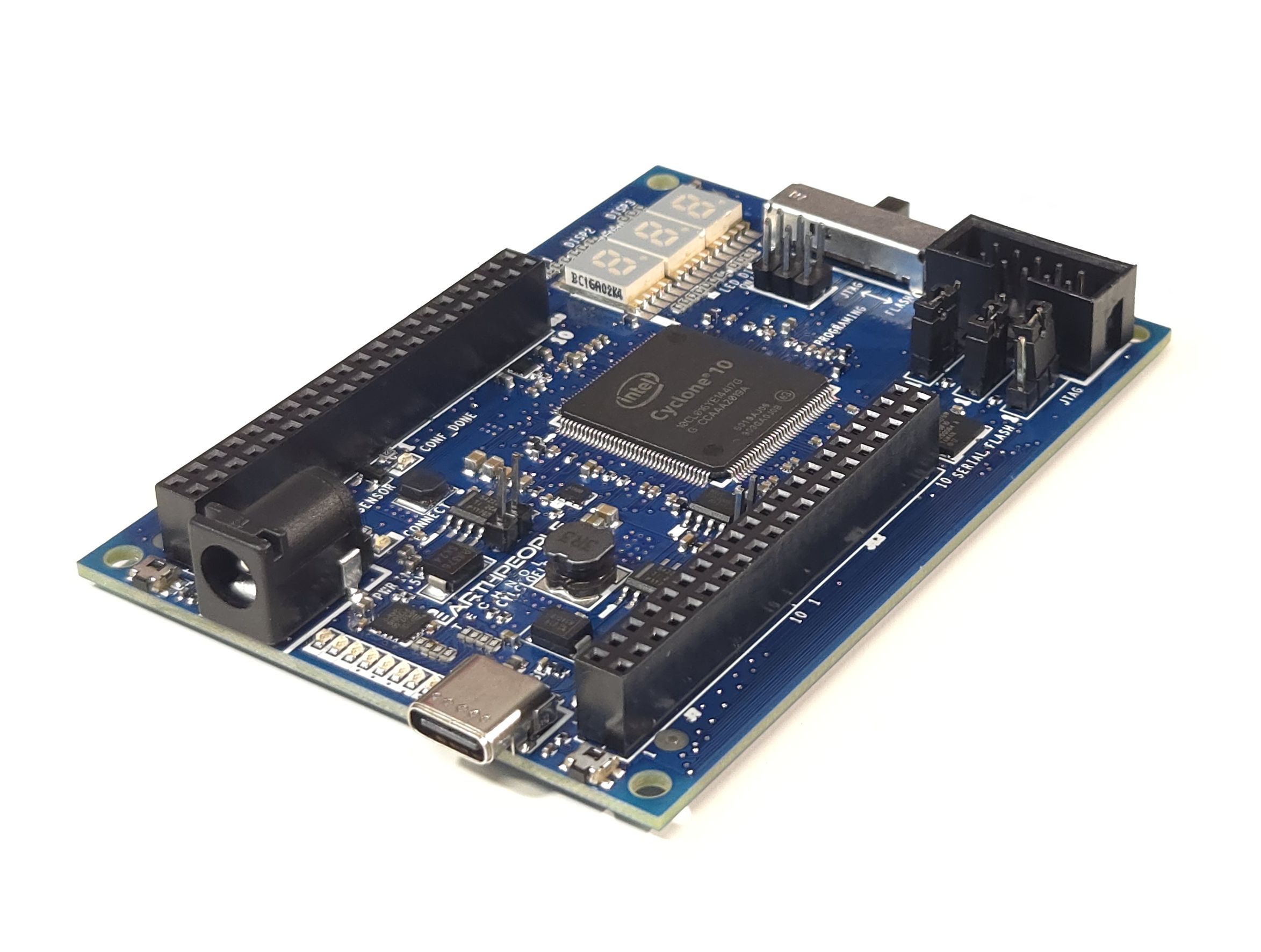
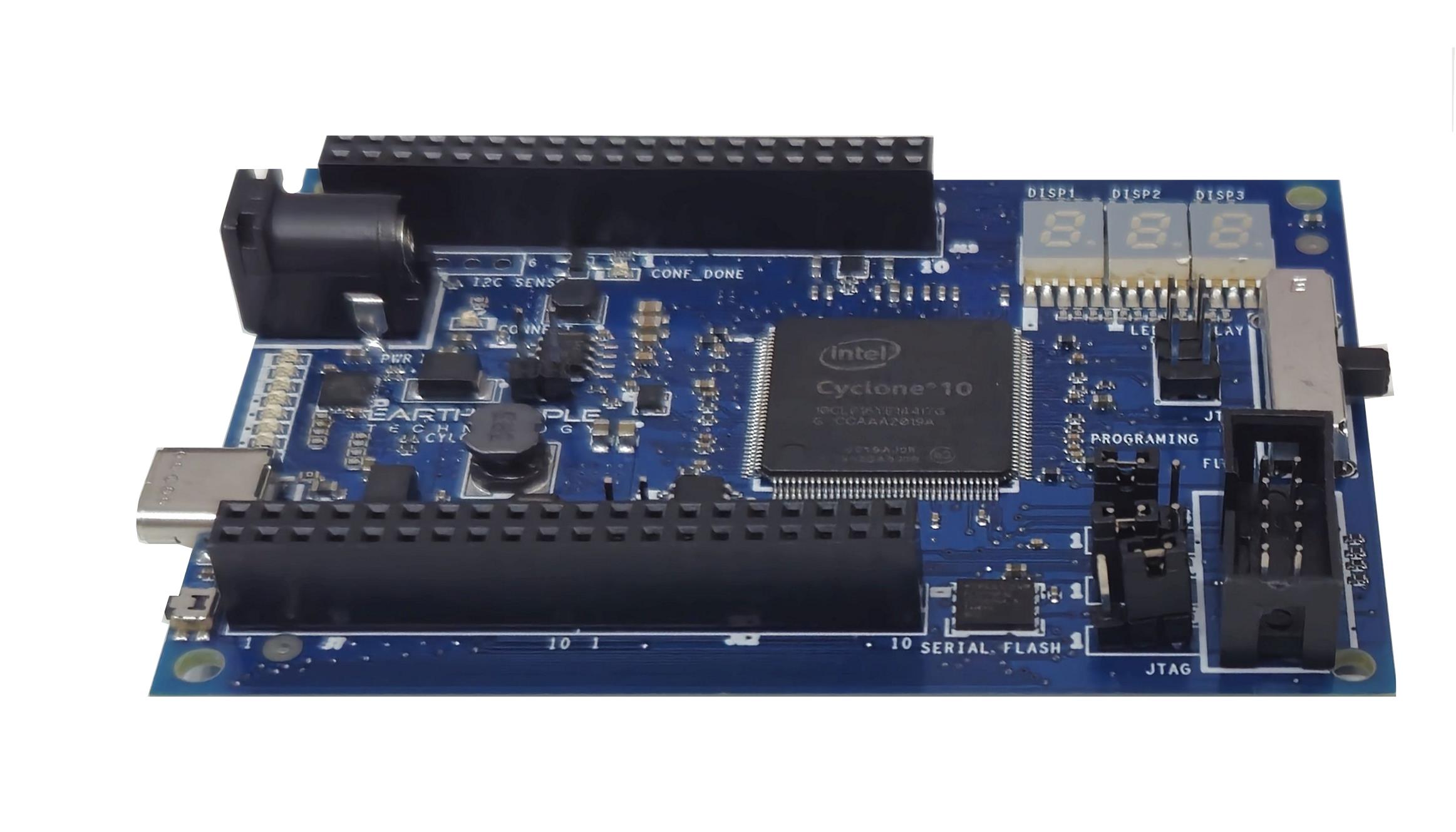
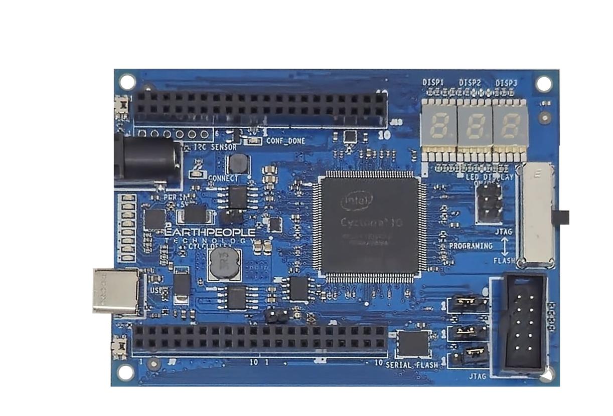
CYCLOFLEX FPGA
DEVELOPMENT BOARD
The CycloFlex is an FPGA development board that is designed for the intermediate
user with some experience designing FPGA projects.
| The CycloFlex is packed with powerful features. The core of the CycloFlex is the Altera Cyclone 10 FPGA. This powerful chip has 16,000 Logic Elements and 504Kbits of Memory. The board includes a 128Mbit Serial Flash chip which allows the board to store up user code for using the FPGA as RISC V soft processor. There are three Green Seven Segment LED Displays, RGB LED and Eight User LEDs. It allows the creation of more diverse projects than beginner projects. |
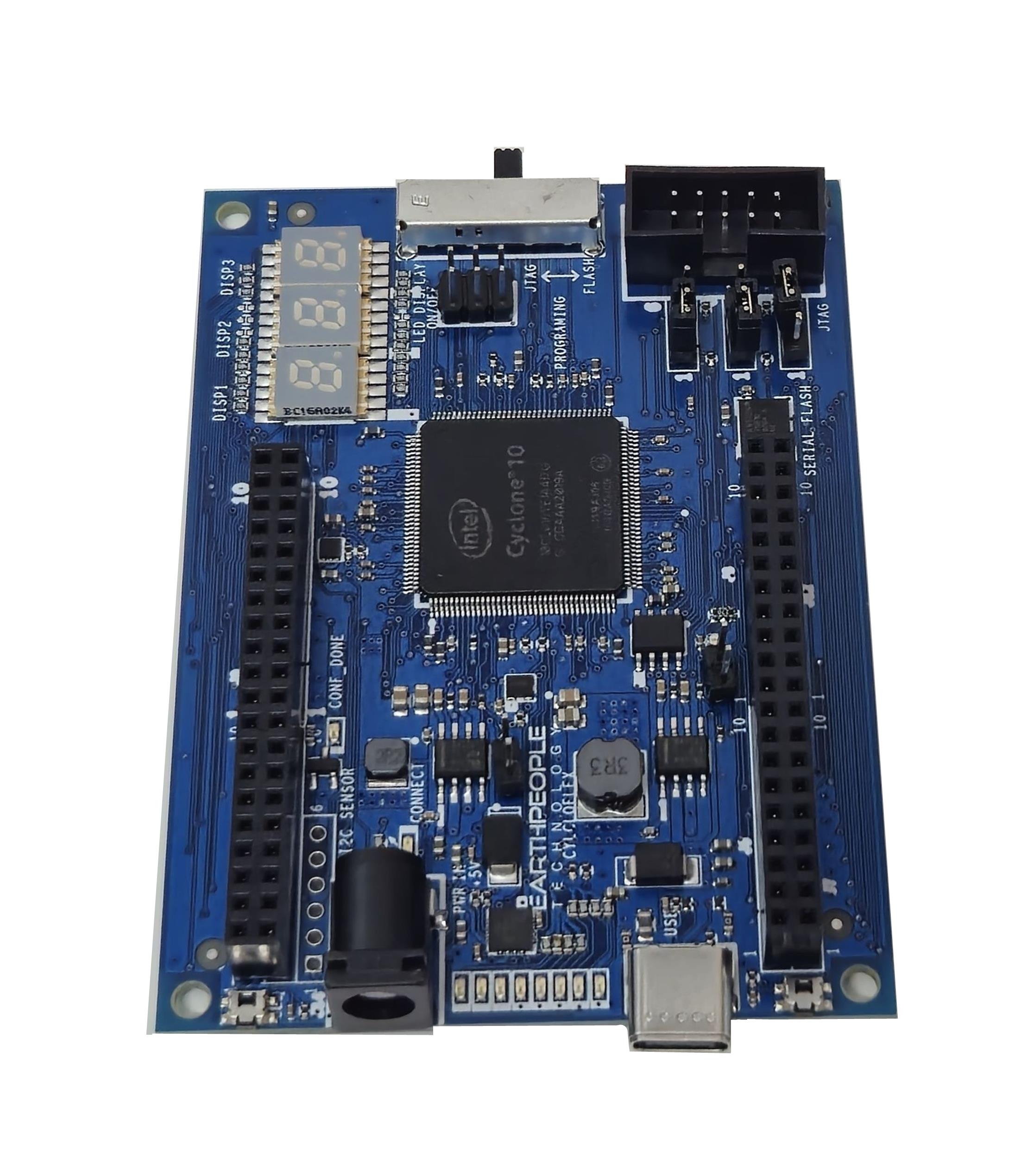
Please Note: The CycloFlex Does Not Contain On Board Programmer.
JTAG Programming and Configuration Flash Programming must be
performed by external Programmer Purchased Separately.
| This board provides a powerful platform for developing and debugging programmable logic code. It has been designed from the ground up to provide the functionality needed for the demanding projects from todays students and hobbyists. The board provides a convenient, user-friendly work flow by connecting seamlessly with Altera’s Quartus Prime Lite software. The user will develop the code in the Quartus environment on a Windows Personal Computer. The programmable logic code is loaded into the FPGA using only the Quartus Programmer tool. |
CycloFlex FPGA Development Board
|
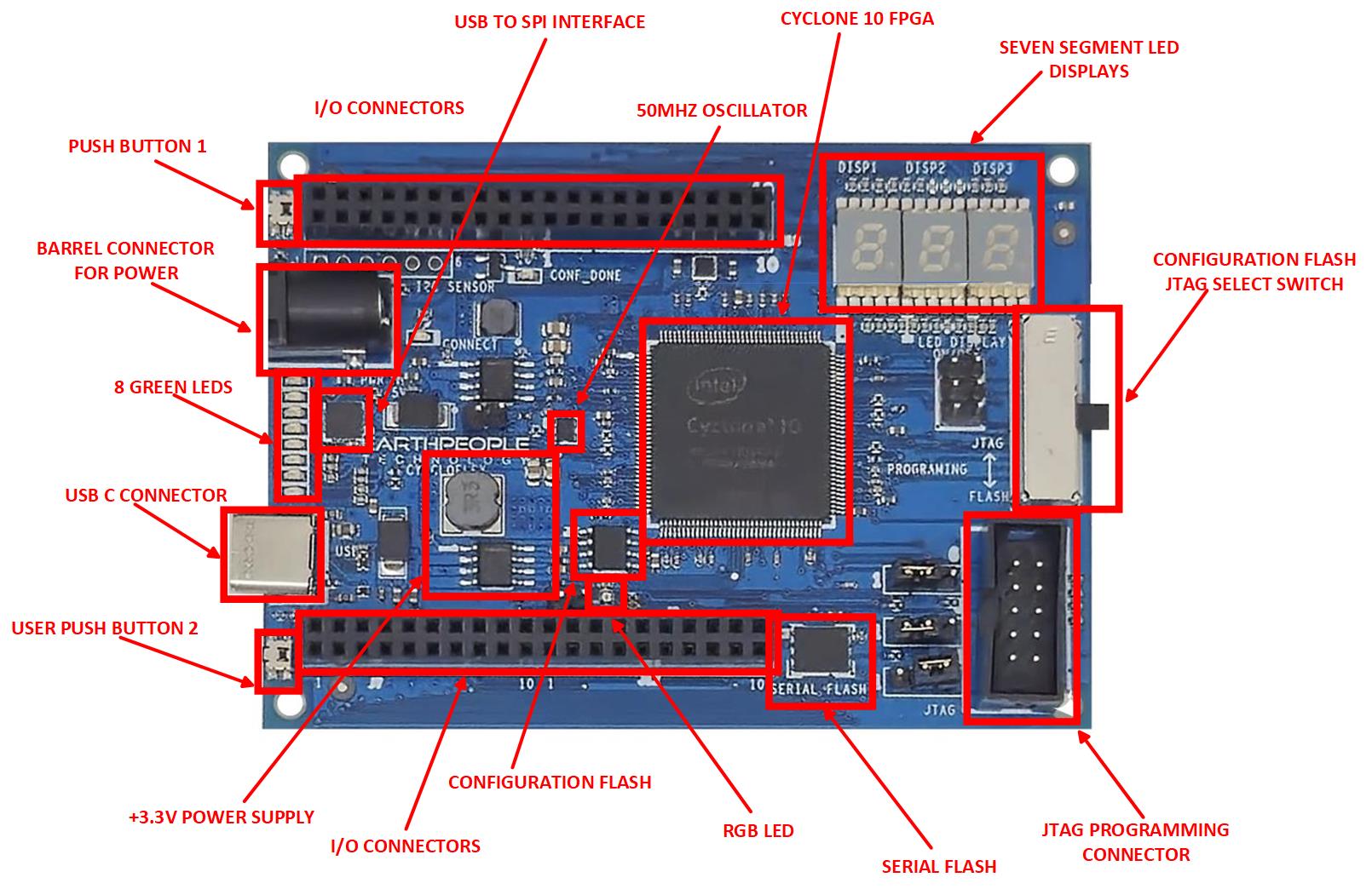
Two Programming Options on the CycloFlex
|
The CycloFlex allows the user to choose between Direct JTAG programming using the *.sof file and programming the configuration Flash with a flick of a switch.
Configuring the Cyclone 10 FPGA on the CycloFlex is the process of
Direct JTAG access allows the Quartus Prime Lite software to program the
The Cyclone 10 FPGA requires configuration before it can be used to perform
|
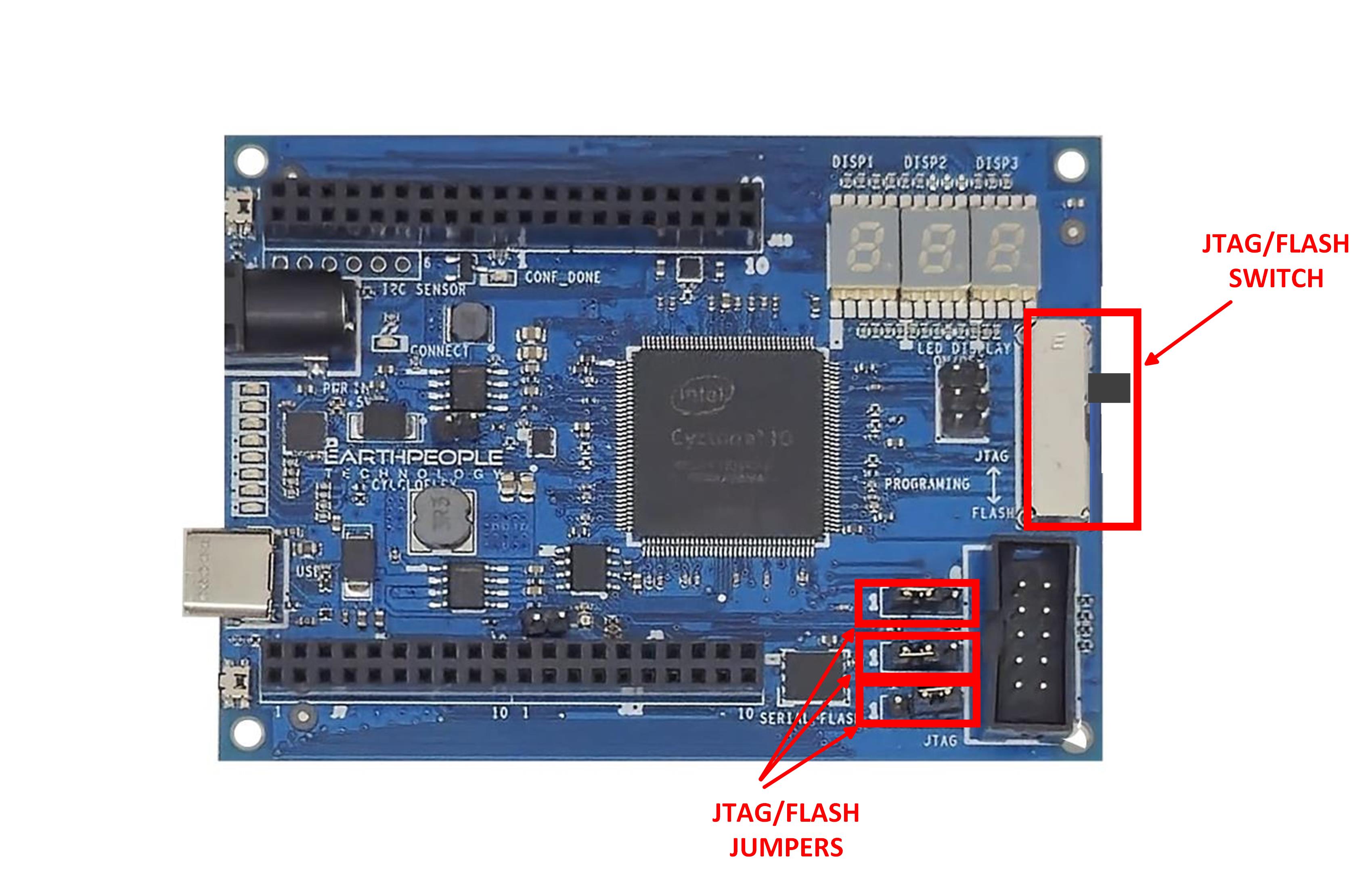
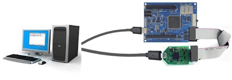
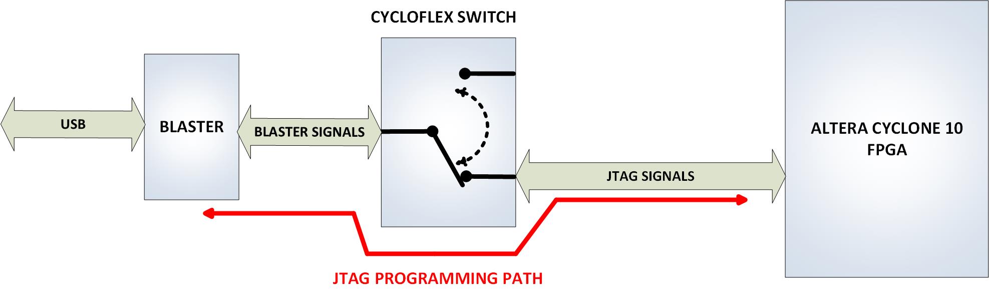
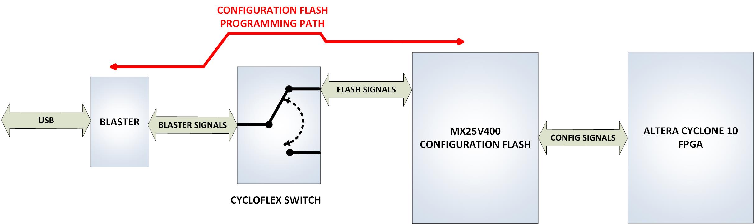
CycloFlex Communications
| The CycloFlex has an on board USB to SPI Serial FTDI chip to connect directly to the FPGA. This chip is the FT220X chip which allows a Host PC to communicate with the FPGA. The FT220X chip provides all of the USB protocol and is transparent to the user. The Input/Output side of the chip provides a modified version of the accepted SPI bus. It uses FTDI’s proprietary FT1248 protocol.
Earth People Technology has created demonstration software that provides a |
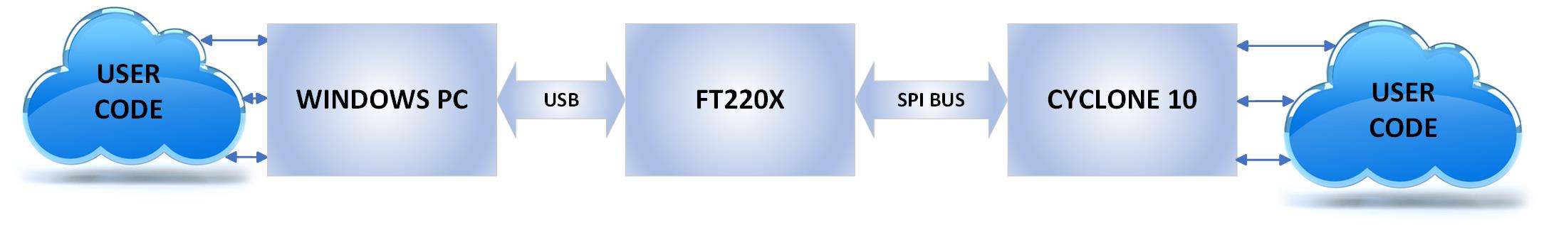
Pre-Loaded With System Demo Software
The CycloFlex board comes pre-loaded with the EPT_System_Demo HDL project in the
FPGA. This project allows the user to test out the functions of the Active Host API
and the board hardware. The software is a multi-function Test Tool which allows the
user to turn On/Off the RGB LEDs, Change the speed/control of the User LEDs, display
characters on the Seven Segment LEDs, test the Push Button Switches and Send/Receive
Bytes from the FPGA. The System Demo Software also has a “Poor Mans Logic Analyzer”
which displays the current status of the Inputs/Outputs at the connectors.
This software demonstrates the USB to SPI communications with the FPGA as well as the
EPT API Active Host Library. All source code and compiled projects are included on the
DVD for the user.
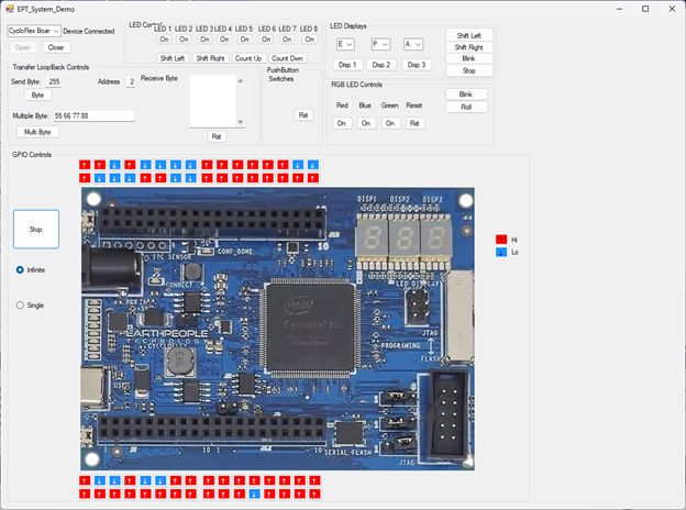
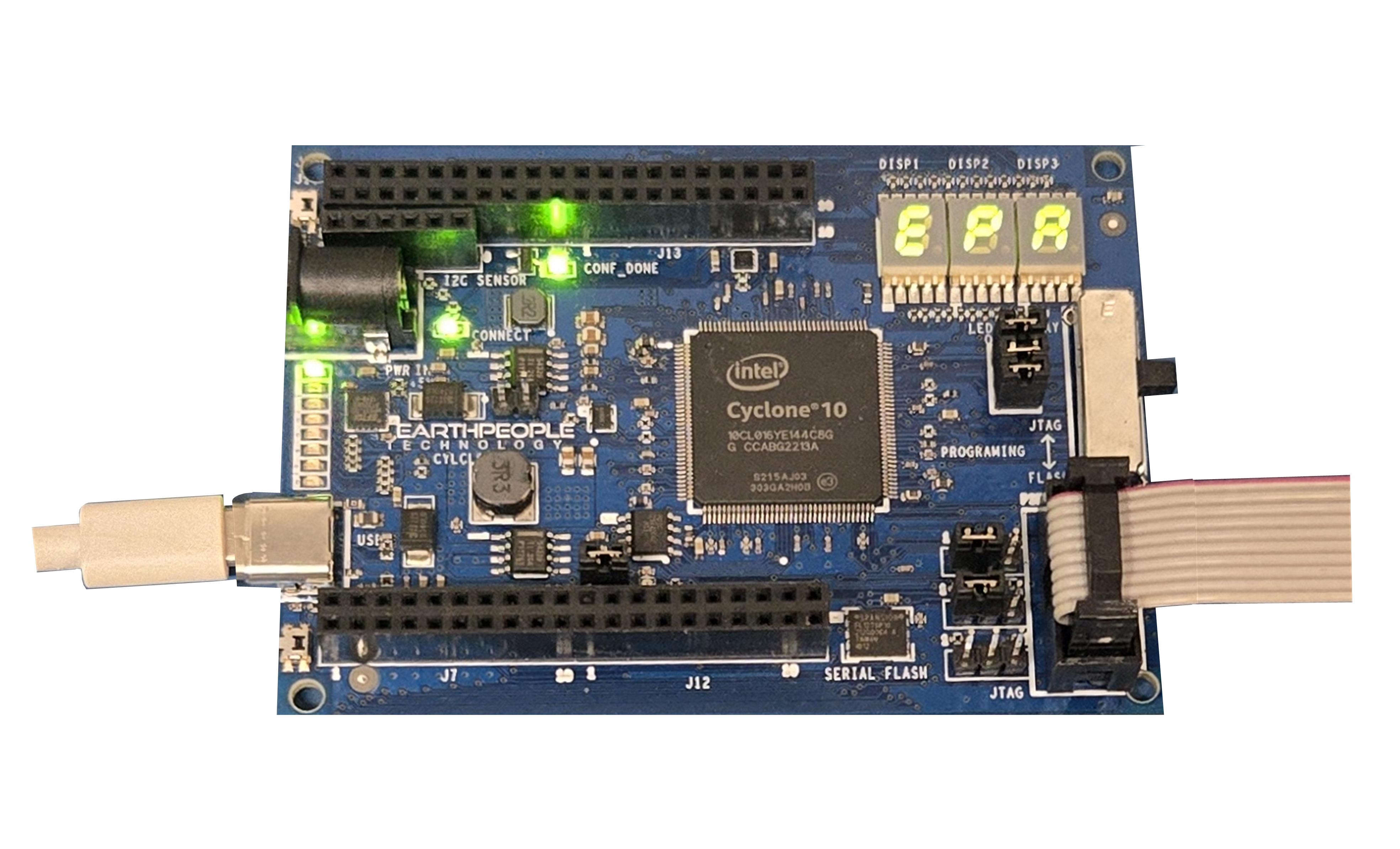
THE CYCLOFLEX HARDWARE
| The CycloFlex is Hardware based on the Cyclone 10 FPGA. The board has 64 Inputs and Outputs connected to 0.1 Inch Headers at the board edge. These are organized as eight 10 pin connectors to allow users to connect to off board circuits. Some of the headers contain +3.3VDC and Ground connections.
The CycloFlex contains three Seven Segment LED Displays. These displays are
The CycloFlex has a Serial Flash chip on the bottom right board. This allows |
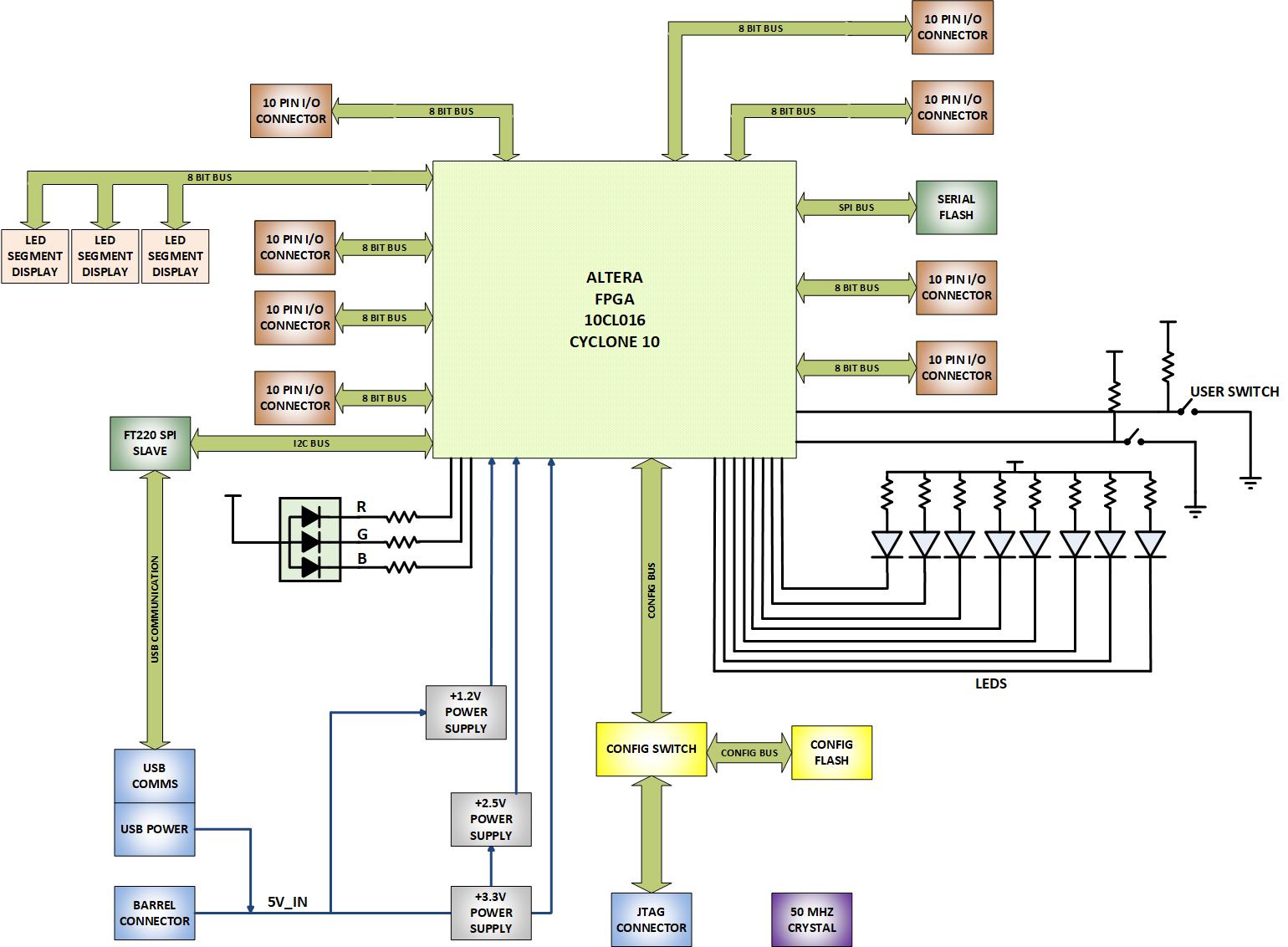
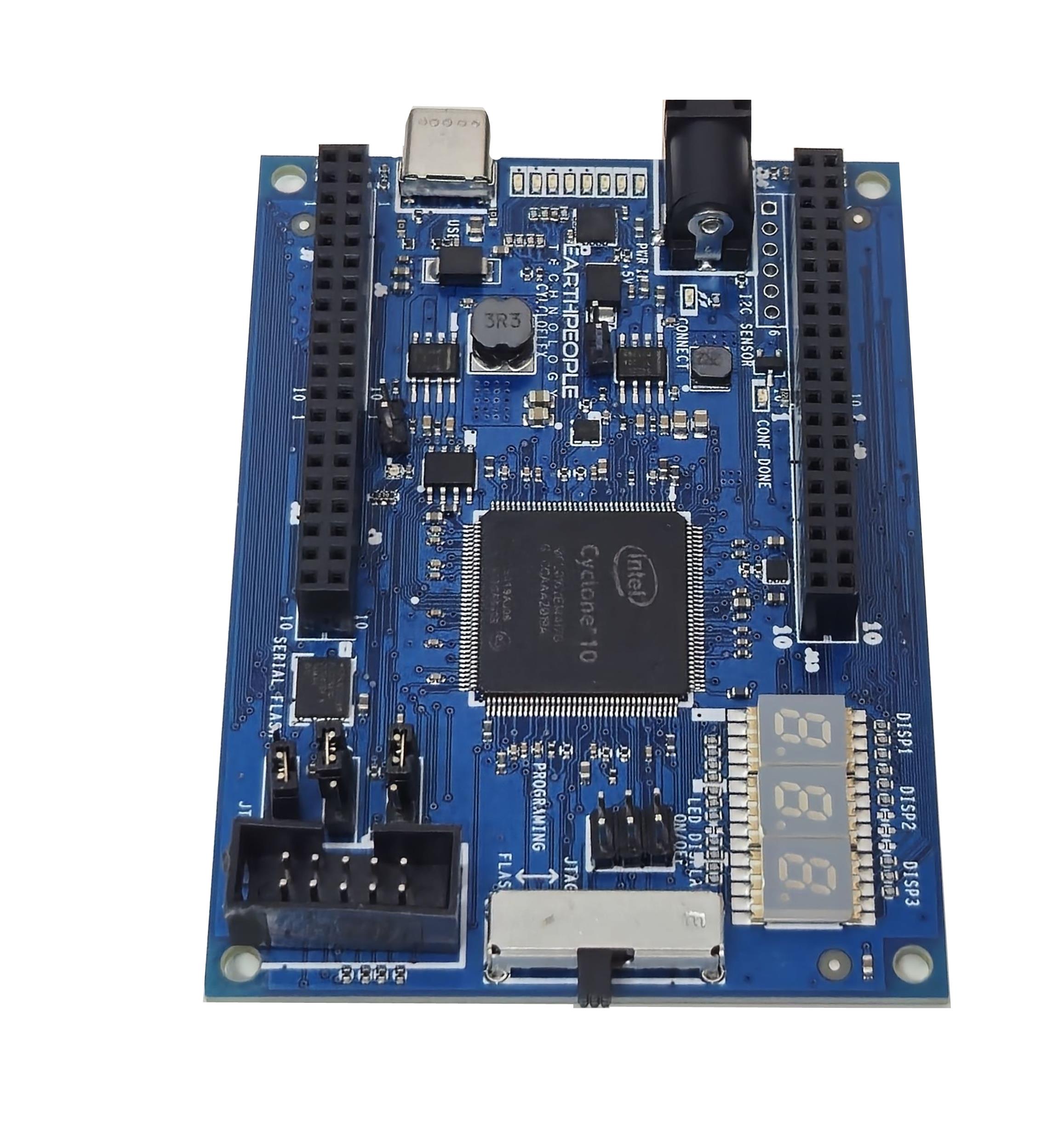
THE CYCLOFLEX AND SIMULATION
| Simulation has always been a weak point for students and hobbyists. Most FPGA beginners write the user code, compile it, synthesize it, program the chip then test out the results. While this approach may work for small, simple designs, it quickly becomes a problem with larger projects. As the user code increases in complexity, better development tools are required to quickly isolate problems. The premier method for this is functional testing.
ModelSim/Questa is included Free with the Quartus Prime Package. ModelSim/Questa is a |
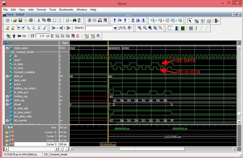
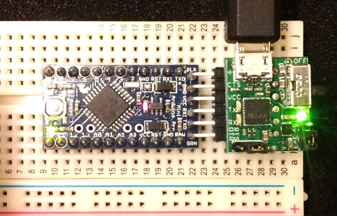
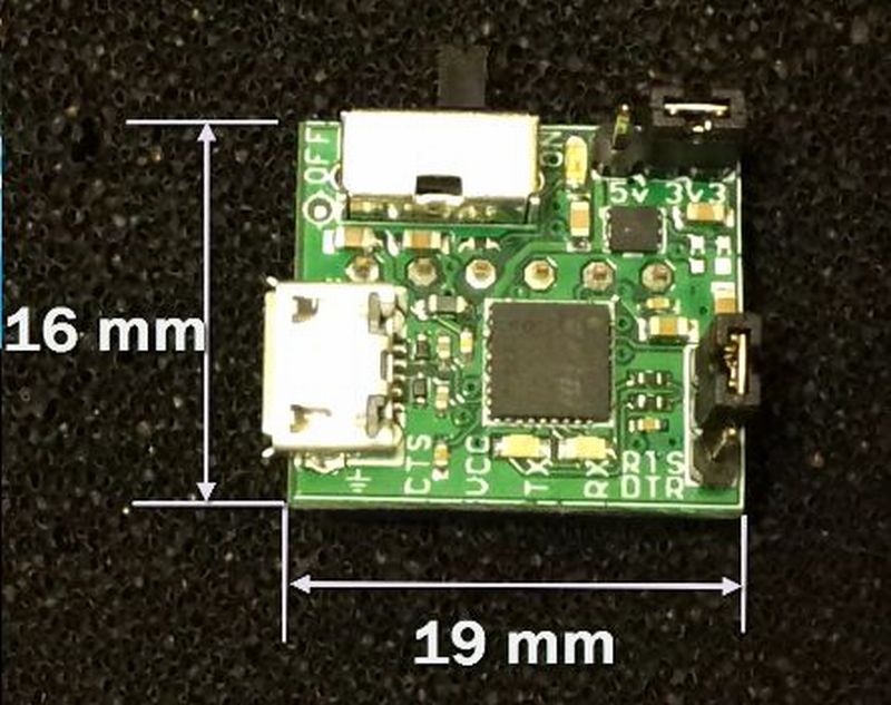
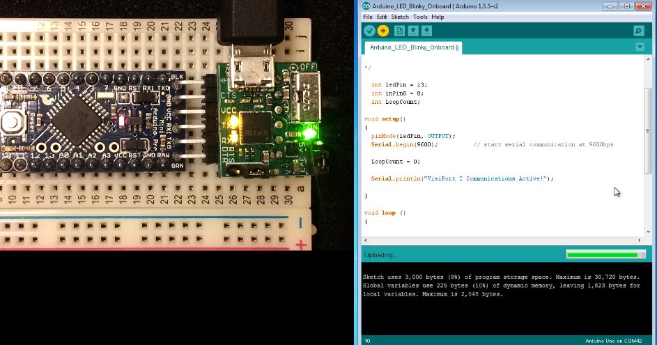
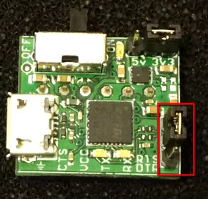
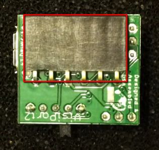
|
| In short, the CycloFlex will cut the time to get the time to get up and running significantly. We also include several pre-made, fully compiled, fully synthesized projects for the user. You can start your project by copying one of these premade projects and adding user code. |
Downloads
| 85-000113 | CycloFlex FPGA Development System User Manual | CYC_MAX_FPGA_DEV_SYS_UM.pdf |
| 95-000113 | MaxProLogic FPGA Development System Data Sheet | CYCLOFLEX_FPGA_DEV_SYS_DS.pdf |
| 45-000113 | CycloFlex FPGA Development System Project DVD | CYCLOFLEX FPGA PROJECT DVD |
| 55-000113 | CycloFlex FPGA Development System Schematics | CYCLOFLEX SCHEMATICS.pdf |
| 35-000100 | EPT Drivers | CDM212365_SETUP.ZIP |