Products Modules
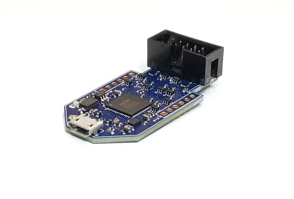
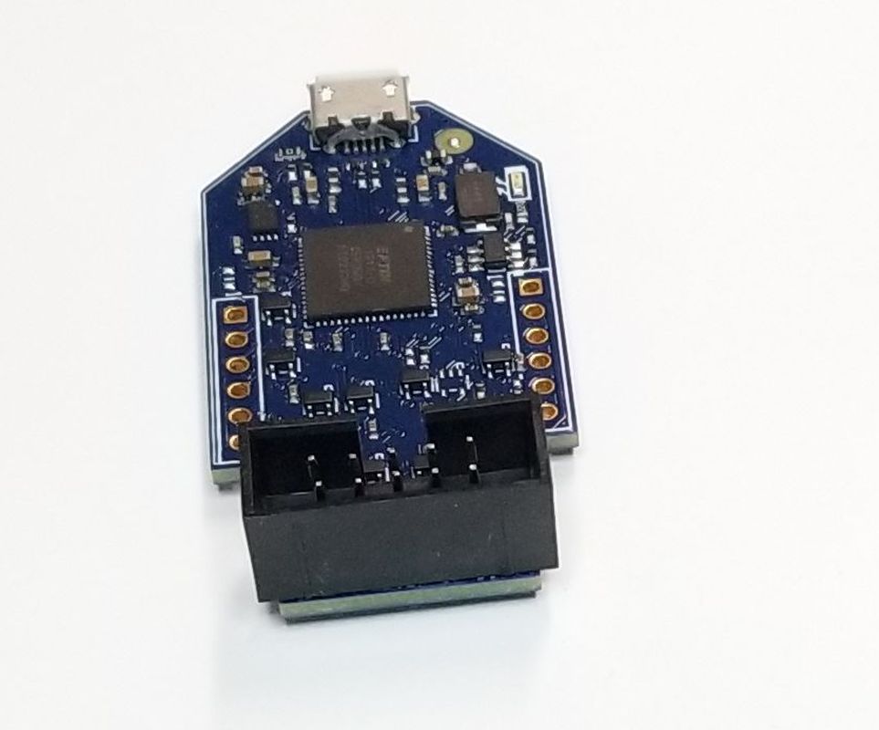
EPT-2232-MM-D2-1
 Dual Channel FTDI Breakout Board
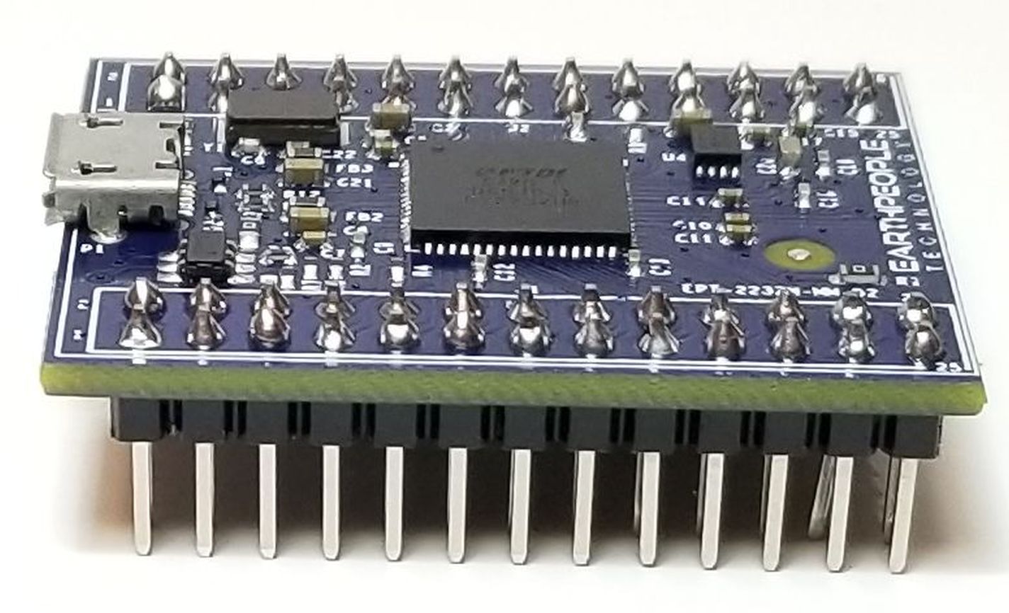
SPECIAL ORDER
30 PIECES OF FTDI BREAKOUT BOARD
TOTAL $599.70
FREE SHIPPING
NO FEES
|
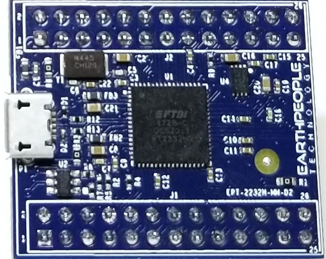
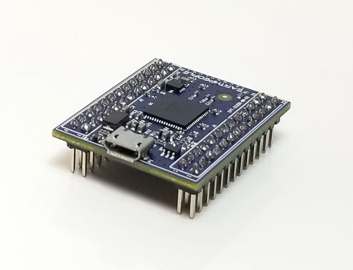
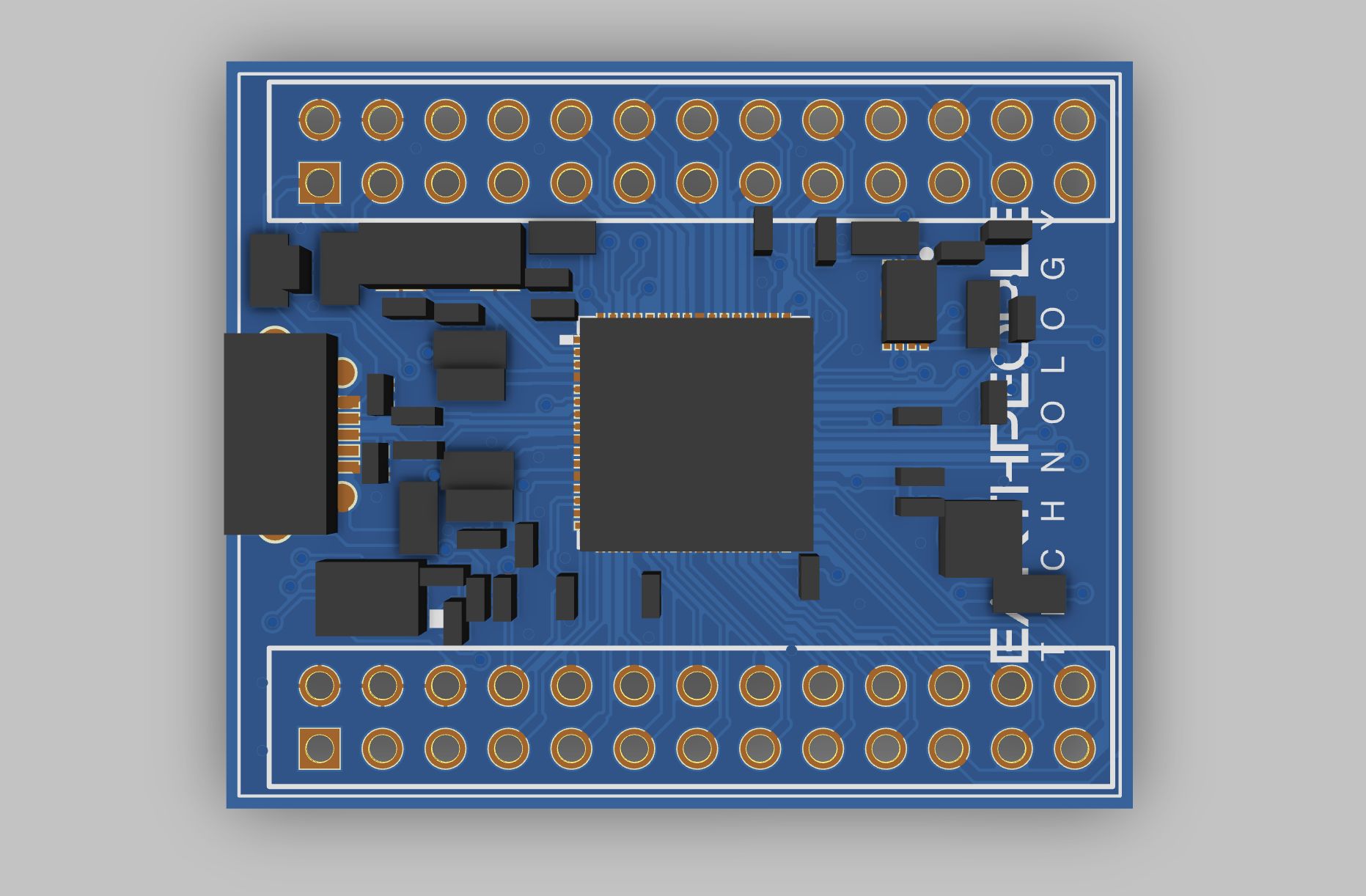
This breakout board is based on the FTDI FT2232H USB 2.0 IO chip. The FT2232H |
|
The FT2232H Breakout Board contains the MPSEE engine. This engine can output SPI, I2C, JTAG or act like an eight bit parallel port. Using the JTAG interface, the FTDI Breakout Board can program the ATMega and Arduinos. It is supported by OpenOCD, urJTAG and others. Hardware Features: |
|
 |
|
The breakout board includes an external EEPROM for custom USB descriptors and VID/PIDs, Serial Numbers, Driver selection (Virtual COM Port or D2XX drivers). There are two 13x2 Headers on 0.1 inch pitch installed on the bottom of the board. An external +3.3V LDO provides power for the FT2232H chip as well as powering off board electronics. The FT2232H chip can operate up to 12MBaud data transfer rates via USB 2.0. It features the USB Micro-B connector. |
Downloads
| 85-000001 | Dual Channel FTDI Breakout Board User Manual | DUAL_CH_FTDI_BREAKOUT_UM.pdf |
| 95-000001 | Dual Channel FTDI Breakout Board DataSheet | DUAL_CH_FTDI_BREAKOUT_DS.pdf |
| 55-000001 | Dual Channel FTDI Breakout Board Schematics | DUAL_CH_FTDI_BREAKOUT_SCHEMATIC.PDF |
| 35-000001 | EPT Drivers | EPT_2.12.00.exe |
EPT-2232H-SP-S1
 JTAG Blaster
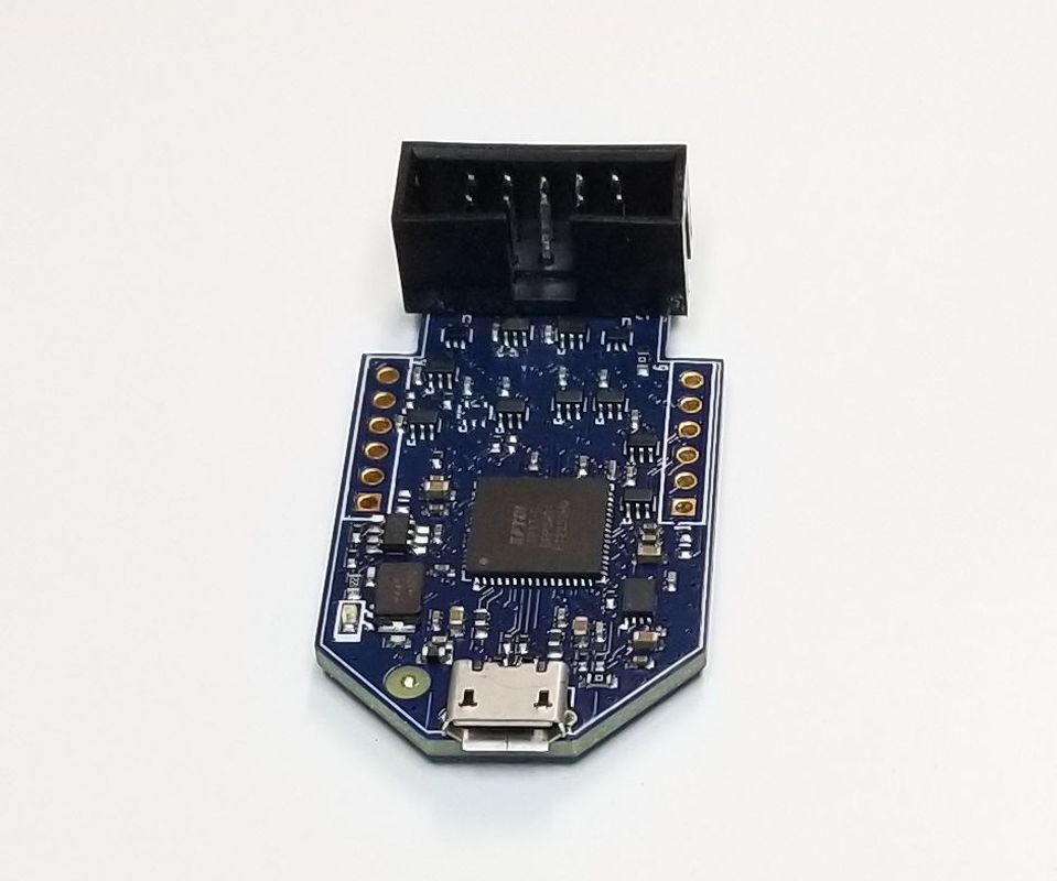
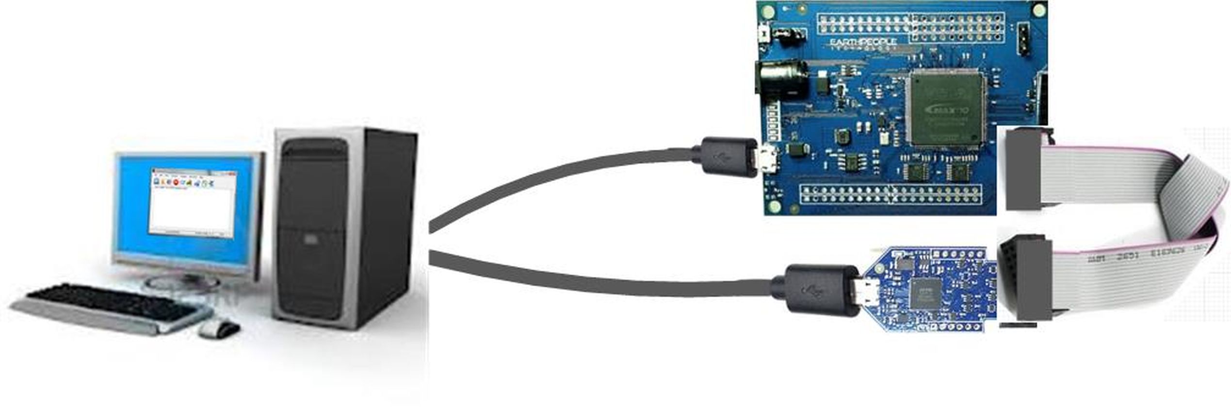
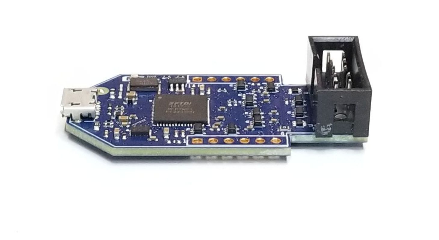
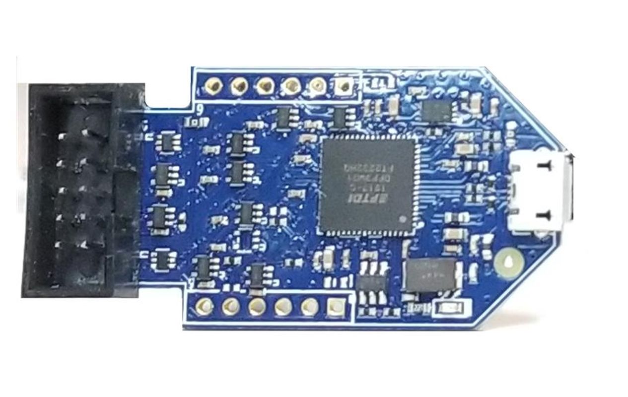
Altera JTAG Blaster Provides JTAG connectivity for Altera devices only |
|
It is designed to program CPLDs and FPGAs from Altera only. It allows JTAG connectivity of any target device voltage from +1.2V to +5V. The Altera JTAG Blaster is compatible with Windows PCs Only. It is not compatible with Linux. |
Program CPLDs and FPGAs
|
The driver provided by Earth People Technology allows this board to be used by the Quartus Application Programmer. Once this driver has been successfully installed, the device can be found in the Hardware Setup drop down box. Just select the device and the programming mode and the appropriate programming file and the board will program your device. |
|
This device connects to an open USB port on a Windows PC and allows the Quartus Programmer application to directly program Altera devices. Installation of the EPT-JTAG- Blaster Driver is required for this device. |
Specifications:
|
| The 5x2 connector has the same pinout as Altera Blasters. |


Downloads
| 85-000012 | EPT JTAG Blaster User Manual | EPT_JTAG_BLASTER_UM.pdf |
| 95-000013 | EPT JTAG Blaster Data Sheet | ALTERA_JTAG_BLASTER_DS.pdf |
| 45-000013 | EPT JTAG Blaster Project DVD | JTAG_BLASTER_GETTING_STARTED_GUIDE.pdf |
| 55-000013 | EPT JTAG Blaster Schematics | EPT_2232H_SP_S1_V2_SCH.pdf |
| 35-000013 | EPT JTAG Blaster Driver | jtag_hw_mbftdi_blaster64.dll |
| 35-000100 | EPT Drivers | CDM212365_SETUP.ZIP |
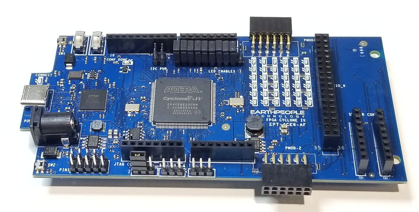
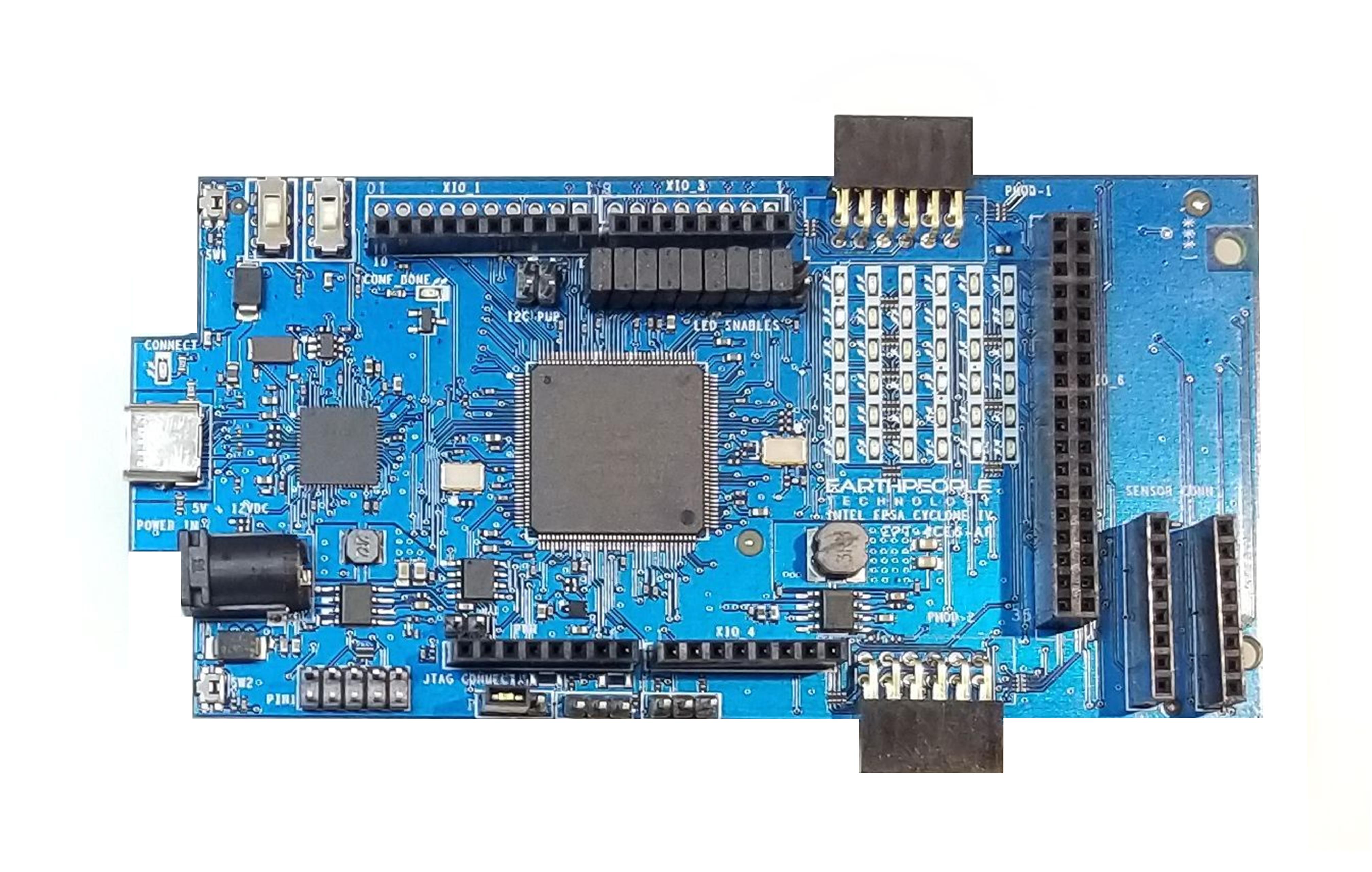
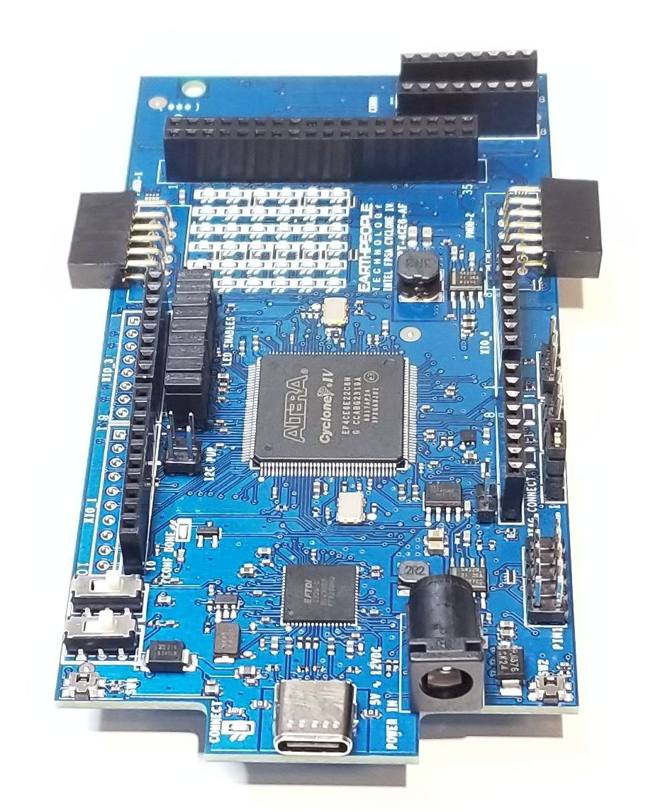
DueProLogic USB-FPGA Development System
ALTERA
CYLONE IV FPGA
DEVELOPMENT
SYSTEM
The DueProLogic is a complete FPGA
Development System designed to easily
get the user started learning and
creating projects.
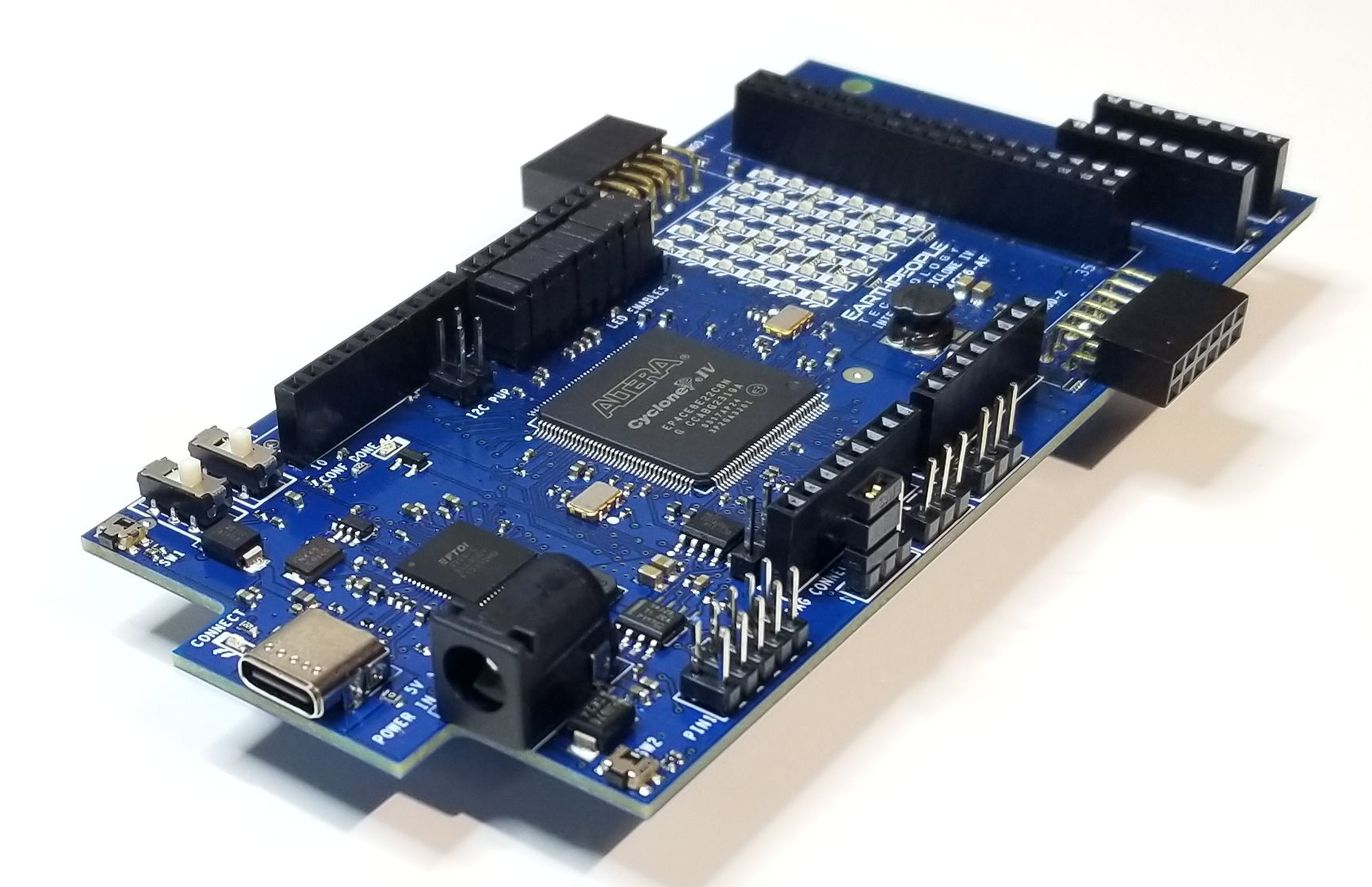
| The DueProLogic makes programmable logic easy with an all inclusive development platform. It includes an Intel/Altera Cyclone IV FPGA, on board programming, four megabit configuration flash, and an SD connector for add on memory. You can create your HDL code, program it into the flash and interact with the hardware via a Windows PC. |
| This is the FPGA (Field-Programmable Gate Array) development board and runtime environment you have been waiting for to get started with programmable logic. |
DueProLogic FPGA Development System
| The DueProLogic (DPL) and its integrated development and distinctive runtime environment has been specifically designed for Electrical Engineering students, hobbyists, and entrepreneurs prototyping/developing/running projects involving logic, with the added opportunity, should it be needed for your project, of readily mating with a widely used microprocessor board, the Arduino Due, and other ARM Cortex compatibles. The combination of FPGA programmable logic and microcontroller is unbeatable in an educational student learning setting and in many other projects where each can bring its strength. |
FPGA Training
| The DPL gives learners the opportunity to have an appropriate hands-on approach when learning logic, exploring different iterations of schematic/code designs with simple uploads of the design, and the operation of those circuits with relatively easy runtime passing of project parameters and data, and an abundance of headers that can interface to external components, without having to spend inordinate amounts of time reading datasheets, designing the right combinations of gates on multi-gate chips, and building/revising/debugging/revising repeatedly… spaghetti bowls of wires and chips on multiple breadboards to connect to those same external components. With the DPL’s FPGA, projects can also more easily be attempted which rely on asynchronous, exceedingly fast, and even multiple separate concurrent logic structures operating in parallel which would have traditionally required a plethora of chip gates or multiple high speed microprocessors to implement parallel processes. Logic circuits are implemented within the FPGA at few- nanosecond gate speeds and highly parallel in operation, effectively a few hundred MHz; Microprocessors often rely on inherently slower single threaded program loops with interrupt servicing, which is typically much slower. Programmable logic is today’s technology for logic learners and implementers, replacing discrete logic chips. |
FPGA Projects
| The DPL allows the learner to be more productive and better focus on the underlying logic and integration with the non-logic aspects of non-trivial projects. Projects and solving real-world applications might involve: |
|
DueProLogic Overview
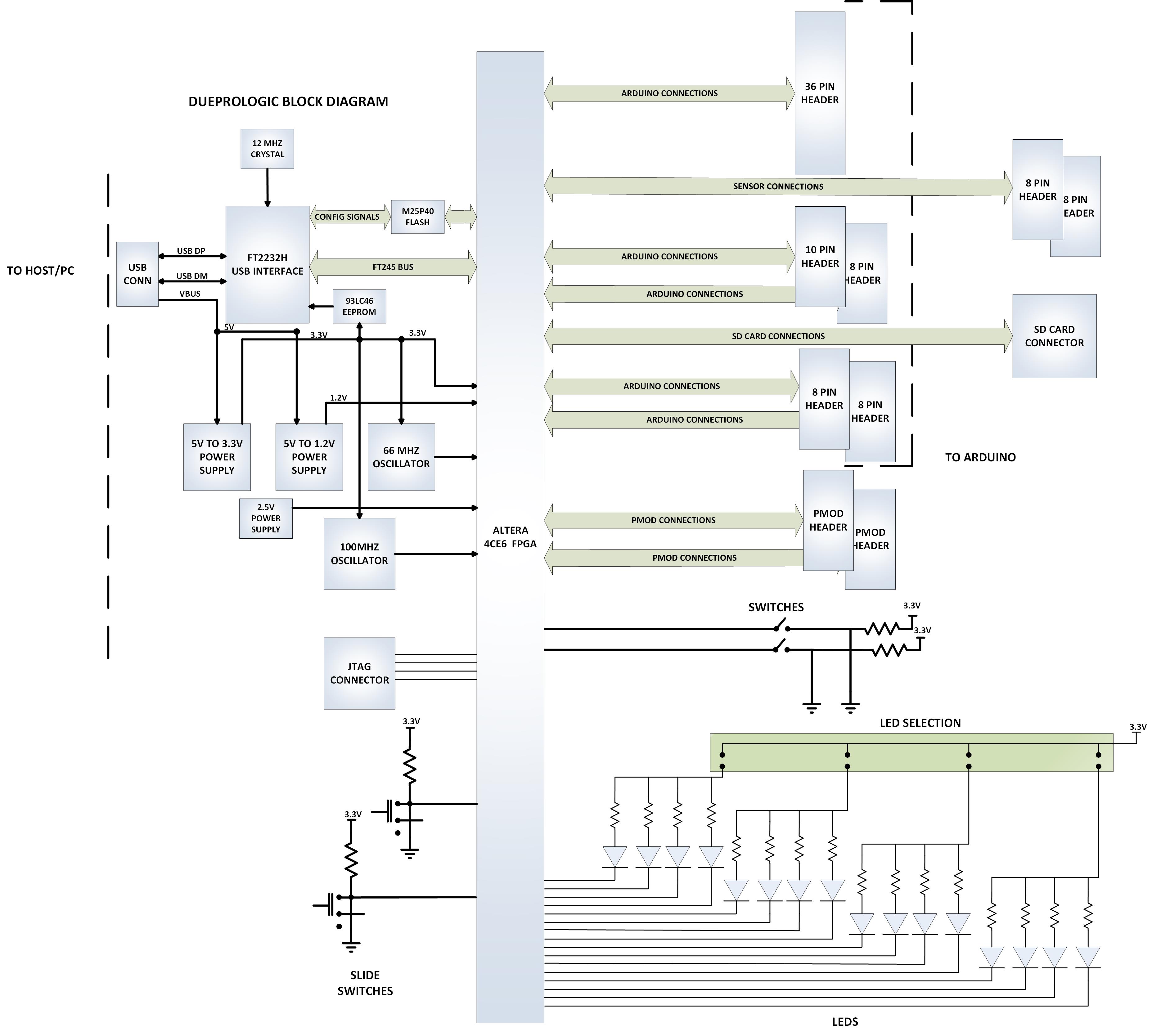
| The DPL is a complete FPGA development environment. It includes a powerful Intel/Altera Cyclone IV FPGA, High-Speed USB interface chip, Full SD Card interface connector, and 4Mb Configuration Flash (for the FPGA). The USB interface chip is an FT2232H with Dual Serial Channels. One channel is dedicated to loading the configuration Flash for the FPGA. The second channel provides a high speed interface for bi-directional communications with the FPGA. Once the configuration Flash is loaded with the users synthesized code, a reset will cause the FPGA to read the Flash and load up the stored image into the FPGA. |
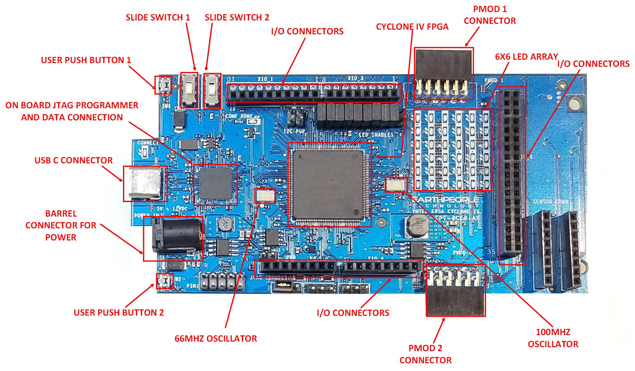
| The block diagram shows all of the parts of the DueProLogic. There are two main power supplies, +1.2V and +3.3V. The +1.2V powers the core of the FPGA while the +3.3V powers the Input/Outputs of the FPGA as well as provides power for user circuits. The DPL contains two oscillators, 66MHz and 100MHz. The 66MHz oscillator is used to provide clocking for the EPT ActiveHost USB communications core. The 100MHz oscillator can be used by the user clocked up using one of the onboard Clock-DLL modules. |
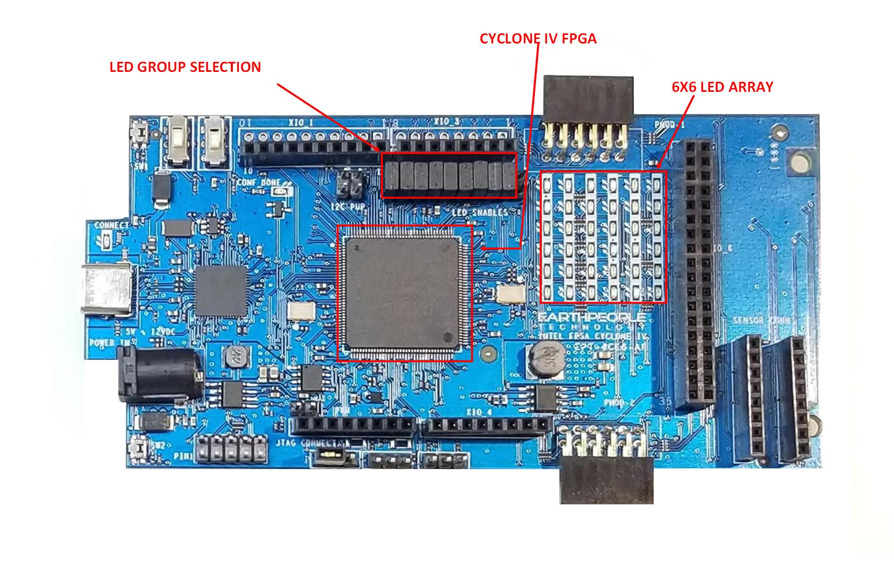
6x6 LED Array
Development Environment
| The DueProLogic includes a 6x6 Green LED array. Each LED is sinked to an individual pin on the FPGA. Each LED is current limited to 6mA. The total current consumed for all 36 LEDs is 216mAs. The FPGA can easily sink this current. So, individually sinking all 36 LEDs makes easy control for User Code. The DueProLogic also contains a method to turn on/off the LEDs in four unit blocks. A jumper is used to control the state of each LED block. |
DueProLogic Block Diagram
Development Environment
| The DPL User Manual comes complete with instructions to set up all the drivers, the Intel/Altera Quartus development environment, and get started creating FPGA projects. The User Manual walks the user step by step from start to finish of the first FPGA project. |
| The included Windows development environment kit includes: Quartus Prime Lite for compiling user code, assigning pins, project setup, programming and other items. The kit also includes the EPT ActiveHost core for the DPL, to facilitate communication between the PC and DPL while the DPL is running a developed project. The kit also EPT has developed a .dll that allows Quartus Prime Lite to directly program the DPL in the same way USB-Blaster works with other Intel/Altera populated development boards. |
|
Configuring the FPGA
| The FPGA on the DPL can be programmed with the HDL project created by the user. Configuration is quick and easy. All that is required is a standard USB cable with a Micro Type B connector, and the EPT Blaster Driver DLL installed on the PC. There are no extra parts to buy - just plug in the USB cable and connect the DueProLogic to the PC. |
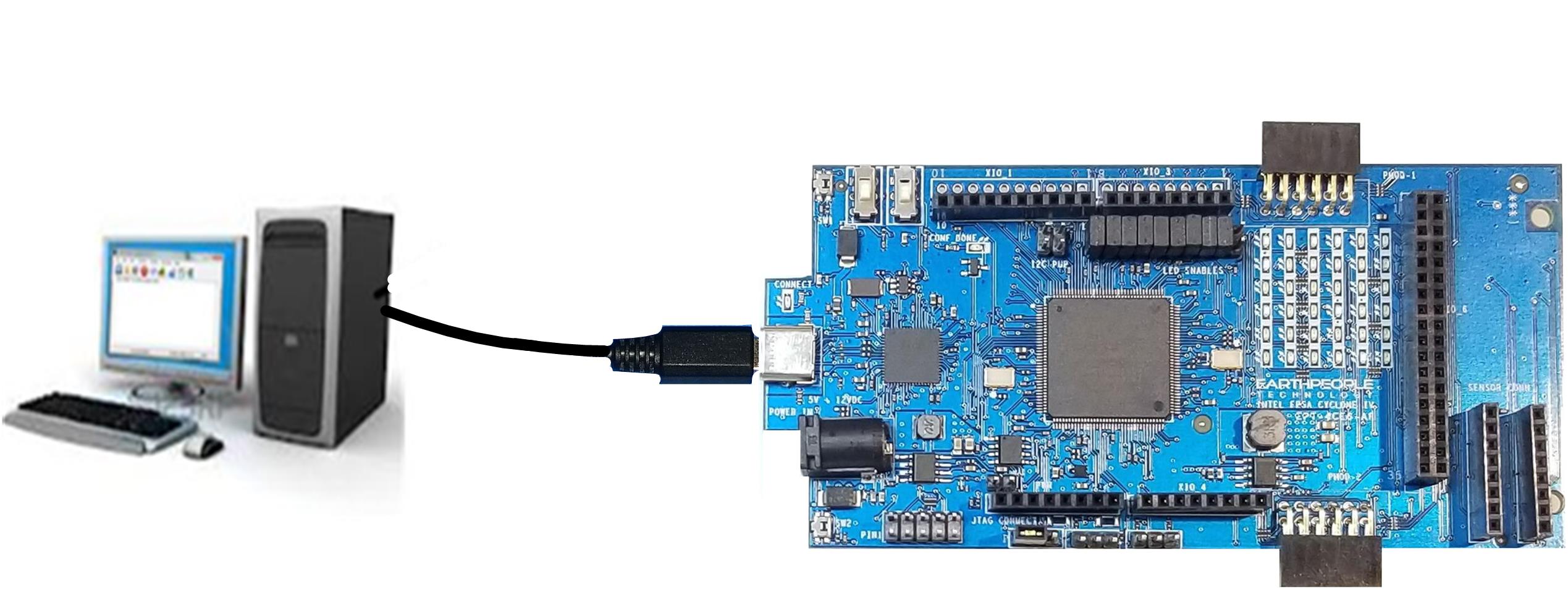
| The DPL Configuration Flash is programmed using the Quartus development environment and the EPT Blaster Driver. Once the the Configuration Flash is programmed. A reset will cause the FPGA to begin configuring itself using the Flash. |
| The board comes preloaded with Blinky, the test that each board goes through before being shipped with conductive foam in a static-control bag. Also included with the product is a DVD with the needed PC/Quartus/DPL drivers, library, User Manual, Schematics, and sample projects, which are also available on the EPT web site. To save expense and possibly the environment, and because many purchasers already have a micro-USB data cable, one is not included. |
| Specifications: Designed to be stand-alone and/or be mated with an Arduino Due. Designed to be inserted directly into a standard breadboard, for easier prototyping Designed with the Arduino Due shield header layout, to accommodate 3.3v-compatible Arduino-type shields, plug-in modules EPT offers, or modules you might develop using standard 0.1” pitch single or double row pin headers. Designed and assembled in the USA and made to be RoHS (no Lead) compliant around the world. The DPL is made to accept standard USB Micro B cable connection and power input of 5-15VDC, but the header logic pins are only 3.3V compatible, like most other high-speed products using today’s chips. Applying 5V to a pin connected to the FPGA chip will cause permanent damage to the FPGA chip. |
DueProLogic Features:
|
Downloads
| 85-000012 | DueProLogic FPGA Development System User Manual | DPL_FPGA_DEV_SYS_UM.pdf |
| 95-000012 | DueProLogic FPGA Development System Data Sheet | DPL_FPGA_DEV_SYS_DS.pdf |
| 45-000012 | DueProLogic FPGA Development System Project DVD | DUEPROLOGIC FPGA PROJECT DVD |
| 55-000012 | DueProLogic FPGA Development System Schematics | EPT-DPL-USB-FPGA-SCHEMATICS.pdf |
| 35-000001 | EPT Drivers | EPT_2.08.24.ZIP |
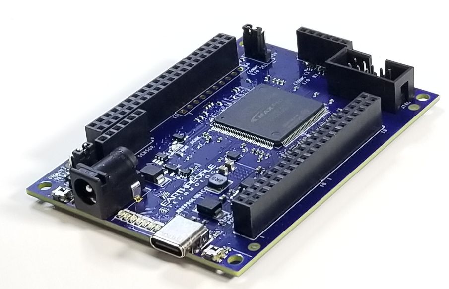
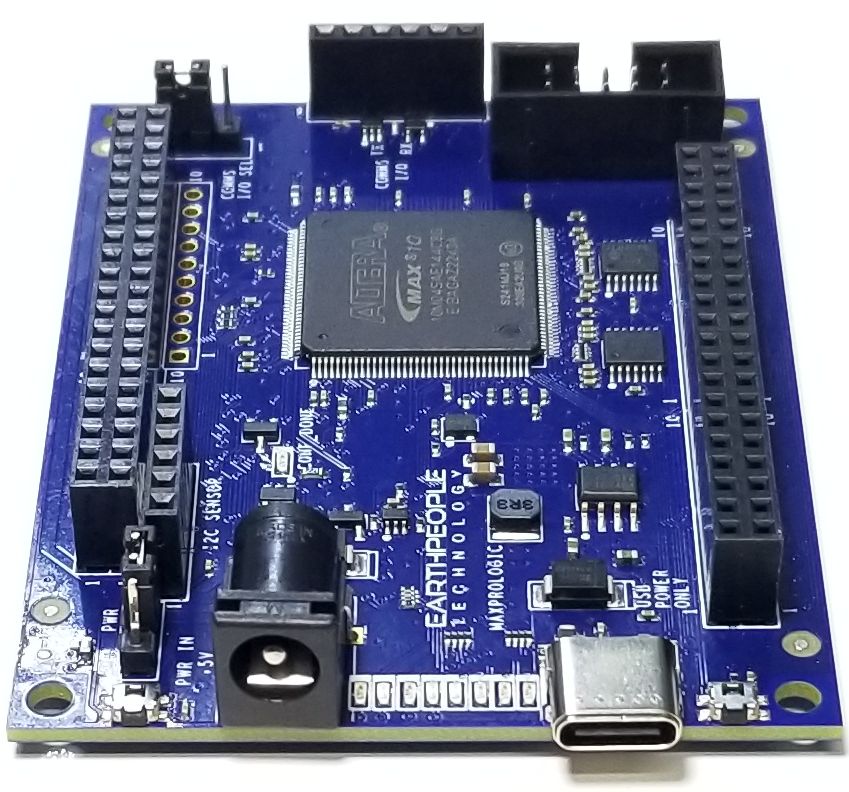
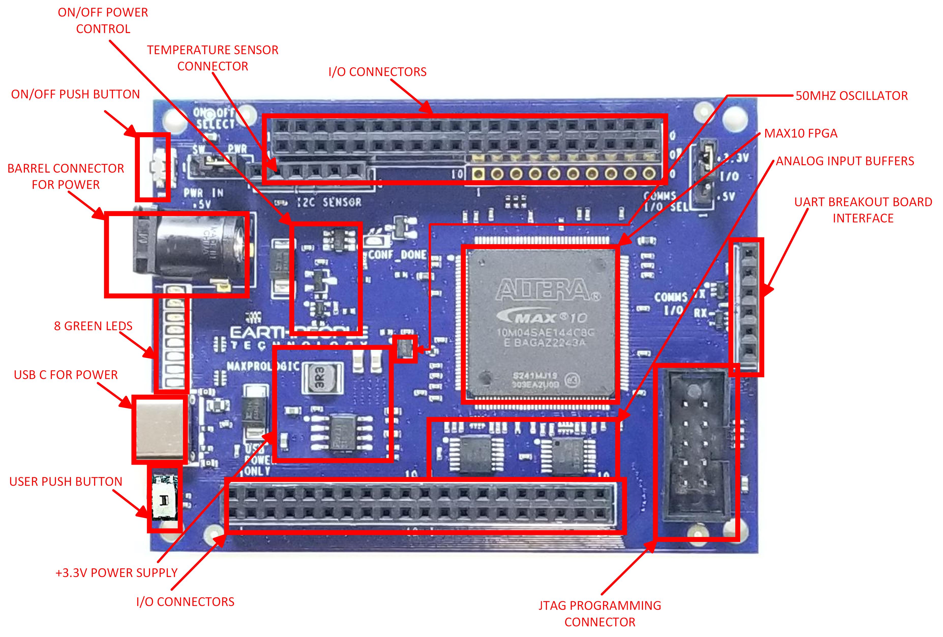
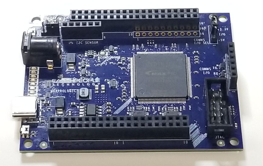
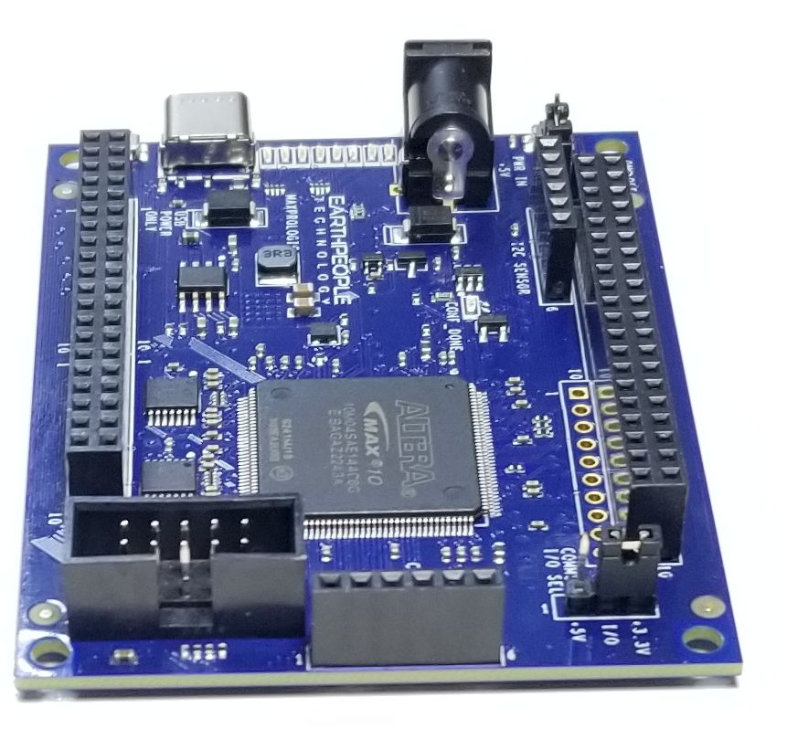
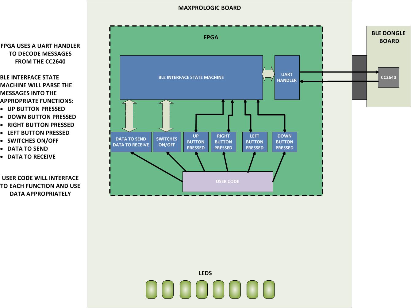
MAXPROLOGIC

|
|
| The MaxProLogic is designed to make digital design easy and cost effective. At Earth People Technology we have years of experience helping students and hobbyists get started with FPGA design. We know that the learning curve in getting started can be a time consuming and frustrating event. So, we created a User Manual that walks the user from unpacking to creating the first project to creating an epic project that will get attention. |
| The core of the MaxProLogic is the Altera MAX10 FPGA. This powerful chip has 4,000 Logic Elements and 200Kbits of Memory. The MAX10 is easily scalable from the entry level college student to the most advanced projects like an audio sound meter with FFT. Upon the many great features of the MaxProLogic is the MAX10 chip has a built |
MaxProLogic FPGA Development System
|
Why the MaxProLogic?
| The MaxProLogic is designed to make digital design easy and cost effective. At Earth People Technology we have years of experience helping students and hobbyists get started with FPGA design. We know that the learning curve in getting started can be a time consuming and frustrating event. So, we created a User Manual that walks the user from unpacking to creating the first project to creating an epic project that will get attention. The Learning Curve with any new piece of hardware is always time consuming. |
|
| In short, the MaxProLogic will cut the time to get the time to get up and running significantly. We also include several pre-made, fully compiled, fully synthesized projects for the user. You can start your project by copying one of these premade projects and adding user code. |
THE MAXPROLOGIC AND SIMULATION
| Simulation has always been a weak point for students and hobbyists. Most FPGA beginners write the user code, compile it, synthesize it, program the chip then test out the results. While this approach may work for small, simple designs, it quickly becomes a problem with larger projects. As the user code increases in complexity, better development tools are required to quickly isolate problems. The premier method for this is functional testing. ModelSim is included Free with the Quartus Prime Package. ModelSim is a powerful tool for finding errors in the user code before you go to synthesis. Earth People Technology has created a guide that walks the user through |
|

PROGRAMMING TOOLS FOR THE MAXPROLOGIC
| The MaxProLogic leverages the Quartus Prime Lite Software for compilation and synethsis. This software tool is completely free and provides very powerful tools for the user. Also included free in the software tools is the simulation tool, ModelSim. A lot beginners to the FPGA world are hesitant about using simulation tools. They feel these tools are too difficult to learn and use. This is where the MaxProLogic breaks that fear. The MaxProLogic comes with a user guide that walks the user from start up to full simulation. Each step is well documented and explained. |
THE MAXPROLOGIC HARDWARE
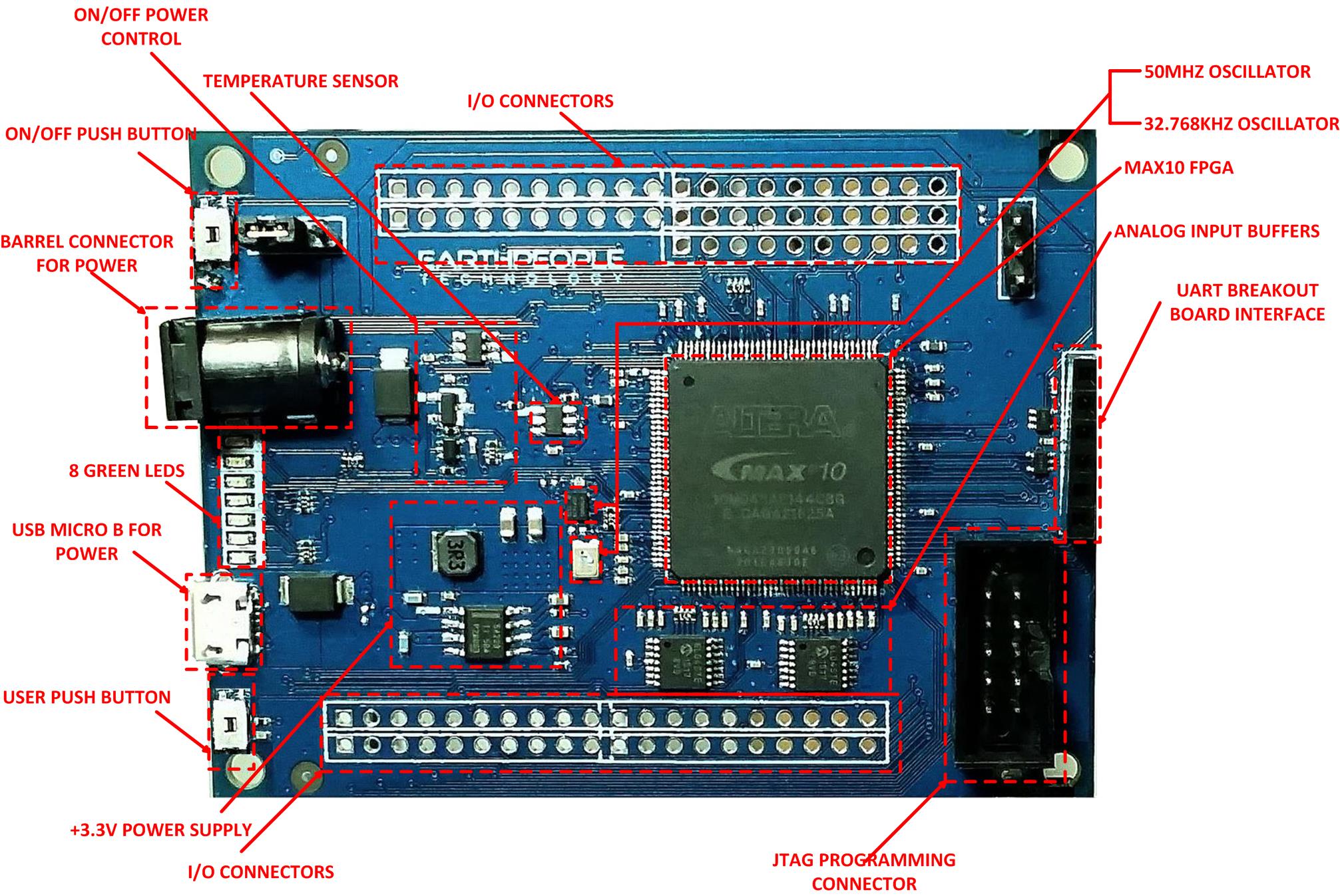
| The MaxProLogic is Open Source Hardware based on the MAX10 FPGA. In addition to the on chip 8 Channel ADC and on chip Flash, the board is loaded with great tools. The board has two power options, standard USB Micro B connector and 5.5mm Barrel connector. You can run the MaxProLogic from a laptop with 2.5W of power. Or you can run it from the +5V @ 2A wall USB chargers for 10W of power. The barrel connector can handle up to +9V @ 3 A for 27W of power. The MaxProLogic has a MicroSD connector on the bottom of the |
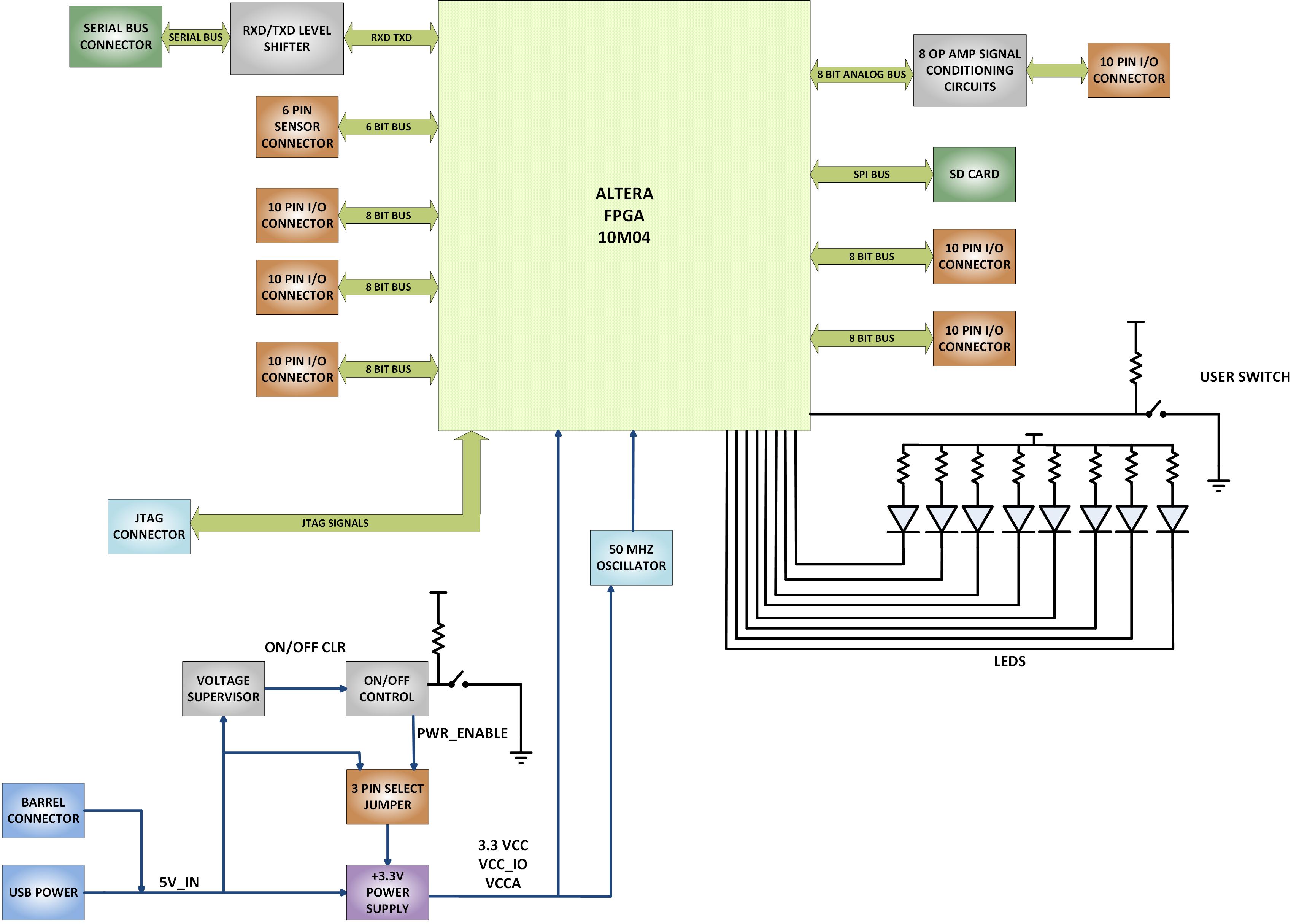
| The block diagram shows all of the parts of the MaxProLogic. There is a main switching power supply for +3.3V. The +3.3V powers the core of the FPGA along with the Input/Outputs of the FPGA as well as provides power for user circuits. |
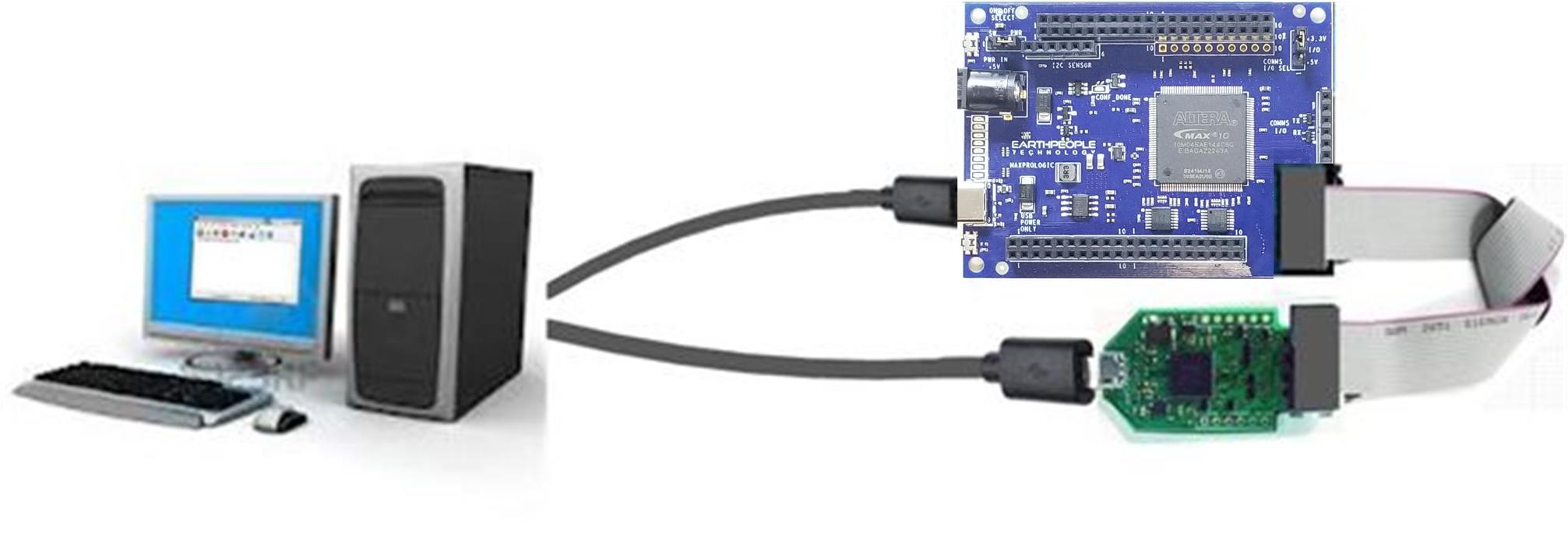
MaxPrologic Communications
| The MaxProLogic has a built in connector to allow FTDI Breakout Boards or Equivalent to connect directly to the FPGA. There are two voltage level translators that allow both +5V and +3.3V devices to communicate via UART with the FPGA. |
Downloads
| 85-000012 | MaxProLogic FPGA Development System User Manual | MAX_FPGA_DEV_SYS_UM.pdf |
| 95-000013 | MaxProLogic FPGA Development System Data Sheet | MAX_FPGA_DEV_SYS_DS.pdf |
| 45-000013 | MaxProLogic FPGA Development System Project DVD | MAXPROLOGIC FPGA PROJECT DVD |
| 55-000013 | MaxProLogic FPGA Development System Schematics | MaxProLogic SCHEMATICS.pdf |
| 35-000001 | EPT Drivers | CDM212364_SETUP.ZIP |
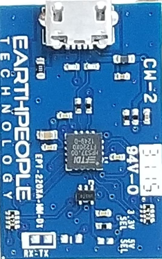
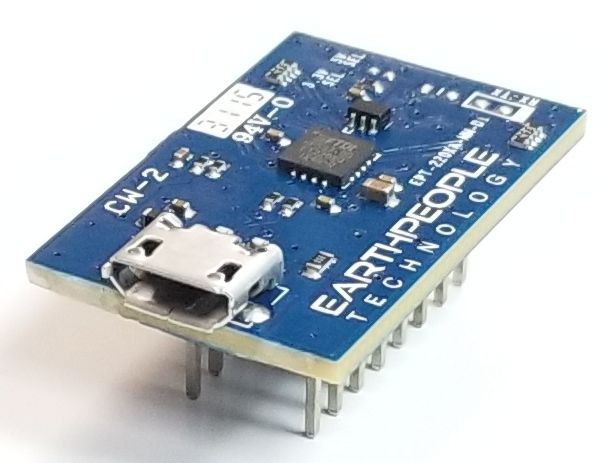
FTDI DUAL CHANNEL BREAKOUT BOARD
Dual Channel FTDI Breakout Board
The FTDI
DUAL CHANNEL BREAKOUT BOARD
|
This breakout board is based on the FTDI FT2232H USB 2.0 IO chip. The FT2232H |
|
The FT2232H Breakout Board contains the MPSEE engine. This engine can output SPI, I2C, JTAG or act like an eight bit parallel port. Using the JTAG interface, the FTDI Breakout Board can program the ATMega and Arduinos. It is supported by OpenOCD, urJTAG and others. Hardware Features: |
|
|
|
|
The breakout board includes an external EEPROM for custom USB descriptors and VID/PIDs, Serial Numbers, Driver selection (Virtual COM Port or D2XX drivers). There are two 13x2 Headers on 0.1 inch pitch installed on the bottom of the board. An external +3.3V LDO provides power for the FT2232H chip as well as powering off board electronics. The FT2232H chip can operate up to 12MBaud data transfer rates via USB 2.0. It features the USB Micro-B connector. |
Downloads
| 85-000001 | Dual Channel FTDI Breakout Board User Manual | DUAL_CH_FTDI_BREAKOUT_UM.pdf |
| 95-000001 | Dual Channel FTDI Breakout Board DataSheet | DUAL_CH_FTDI_BREAKOUT_DS.pdf |
| 55-000001 | Dual Channel FTDI Breakout Board Schematics | DUAL_CH_FTDI_BREAKOUT_SCHEMATIC.PDF |
| 35-000001 | EPT Drivers | EPT_2.12.00.exe |
Odin-Link BLE Plus MaxProLogic Development Kit
|
|
 |
 Odin-Link BLE Plus MaxProLogic Development Kit
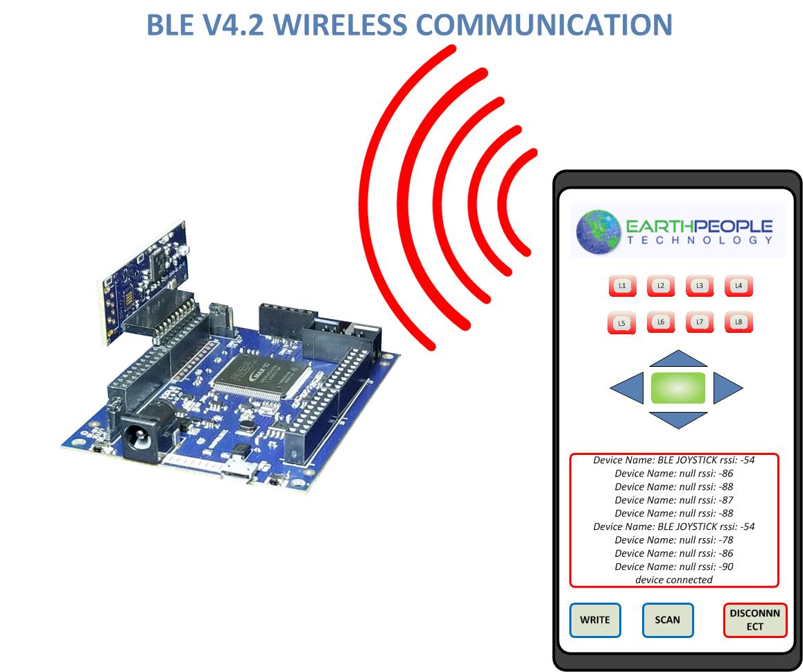
The Odin-Link BLE Plus MaxProLogic Development System
Provides the Easiest Way to Add BLE to any DIY Project.
| The Odin-Link plus MaxProLogic is the simplest BLE development kit on the market. The Android phone app, included with the kit, is completely self contained, there is no programming or third party provider access. Just load the “JoyStick.apk” onto your Android phone and start sending commands to the Odin-Link. Most BLE development kits require a third party provider to build a custom Phone app. Because of this, the user must build the phone app, compile the phone app, then load it onto an Android Phone. |
Kit Contents
| The kit is ready to use out of the box. You will need a USB Micro B cable. |
|
 |
| The JoyStick app is only available for the Android phone. It provides a simple interface to send commands to the Odin-Link board. There are switches to turn lights on and off, buttons to send single commands and a text communication path. Users can build a wide array of DIY projects including remote lamp controller, BLE controlled robot and remote weather station. |
 |
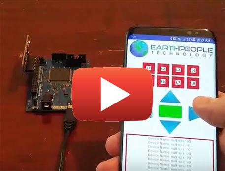 Click For Video Click For Video |
Odin-Link BLE Board
| The Odin-Link BLE board comes pre-programmed with all the profiles required for the JoyStick app to run on an Android phone. No programming is needed for the board. The use of a third party phone app provider to produce a custom app requires programming of the BLE profiles into the BLE chip. This forces the users into writing code, debugging code and programming the BLE chip. The Odin-Link BLE Board development kit eliminates this extra work. It's virtually plug and play. |
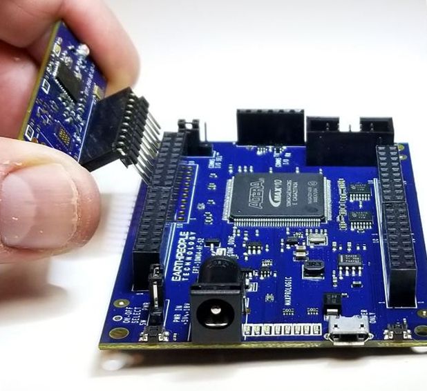 |
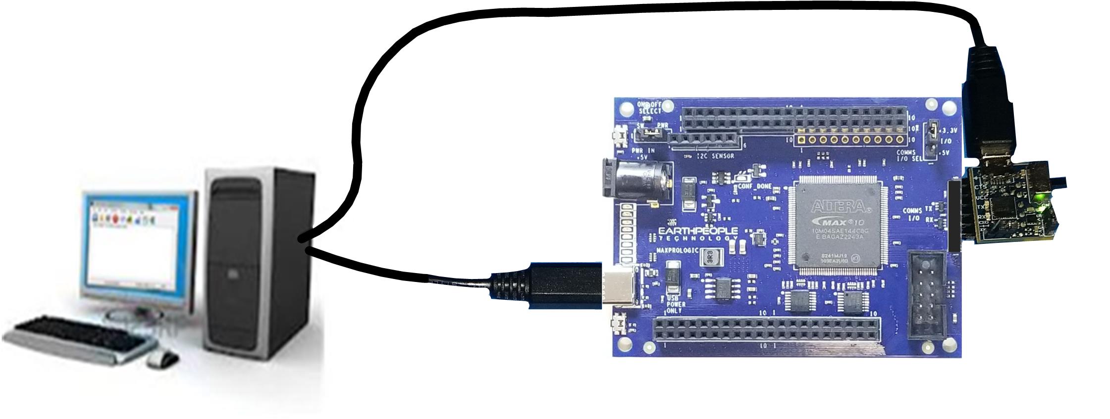
| The Odin-Link BLE board includes a v4.2 BLE chip along with a 2.4GHz antenna and matching network. Texas Instruments provides the CC2640 BLE chip. EPT provided the antenna tuning for maximum RF range. The Odin-Link BLE board plugs directly into the J5 connector of the MaxProLogic. All power and communication happen through through this connector. It communicates with the FPGA over a UART serial link. EPT has created a proprietary Verilog interface that runs in the FPGA and allows full bidirectional communication with the Android phone, via the CC2640 v4.2 chip. |
MaxProLogic FPGA Board
|
The MaxProLogic is an FPGA board with the Intel/Altera MAX10 at its heart. The MaxProLogic is an integral piece of the Odin-Link BLE Plus MaxProLogic development kit. It is a standalone FPGA board that is powered by an external source. The onboard switching power supply provides a stable power source for the Odin-Link BLE board. It has a 50MHz ultra low jitter oscillator to provide an array of different clock sources in the FPGA. The Odin-Link BLE plugs directly into the J5 socket of the MaxProLogic. The serial UART signals are connected directly from the CC2640 to the pins on the MAX10 FPGA. |
 |
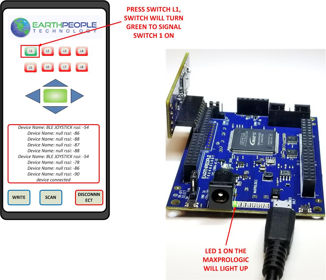
| The JoyStick Android App takes inputs from the user and generates BLE packets. These BLE packets are transmitted from the Android phone and received by the Odin-Link BLE board. The Odin-Link BLE board decodes the packets and produces ASCII generated commands that are transmitted over the serial UART signals to the MAX10 FPGA. |
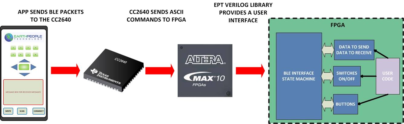 |
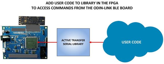
| EPT has created a Verilog library that runs in the MAX10 FPGA to convert the serial ASCII commands into usable signals. The user will interface their code to the library using an easy SDK from EPT. This makes creating advanced projects quick and easy. Just include the library when synthesizing the FPGA project. |
 |
| The Verilog library will parse out each command and send it to the appropriate block interface. There are three block interfaces, buttons, switches and text. There is a demo BLE LED Blinky project included in the DVD. This project allows the user to individually turn on and off the LEDs of the MaxProLogic board. The demo will also allow the user to blink the LEDs in a Blinky Show. The demo project has all the source code, fully compiled project, programming files, and full simulation. |
 |
Downloads
| 105-000001 | Odin-Link + MaxProLogic Development User Manual | ODINLINK_MAXPRO_DEV_SYS_UM.pdf |
| 115-000001 | Odin-Link + MaxProLogic DataSheet | ODINLINK_MAXPRO_DS.pdf |
| 125-000001 | Odin-Link + MaxProLogic Schematics | MAXPROLOGIC_SCHEMATIC.PDF |
| 135-000001 | Odin-Link + MaxProLogic Project DVD | ODINLINK_MAXPRO_DEV_SYS_PROJECT_2.7_DVD.zip |
| 35-000001 | EPT Drivers | EPT_2.12.00.exe |
USB SPI Slave Breakout Board
 USB SPI Slave Breakout Board
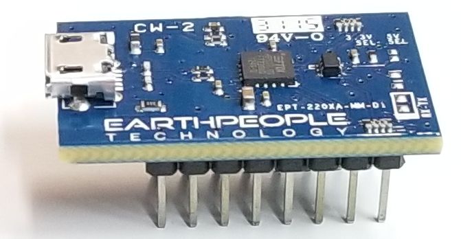
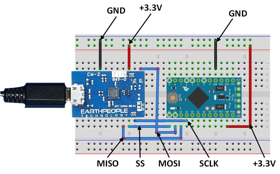
Transfer SPI data directly to the PCThe USB SPI Slave Breakout Board provides a simple interface for bi-directional communication with the PC from any MCU (including the Arduino family). It is designed to connect directly to the standard bread board with a reduced footprint. Once connected to an MCU, the MCU Master SPI bus connects to the FT220X chip. This chip connects the SPI bus to the USB bus. The PC communicates with the USB SPI Slave Breakout Board as COM Port. This allows any simple Terminal Window software (such as TeraTerm) to communicate directly with the MCU. Earth People provides sample software so the user can use the Arduino functions to send data to be graphed on the PC. |
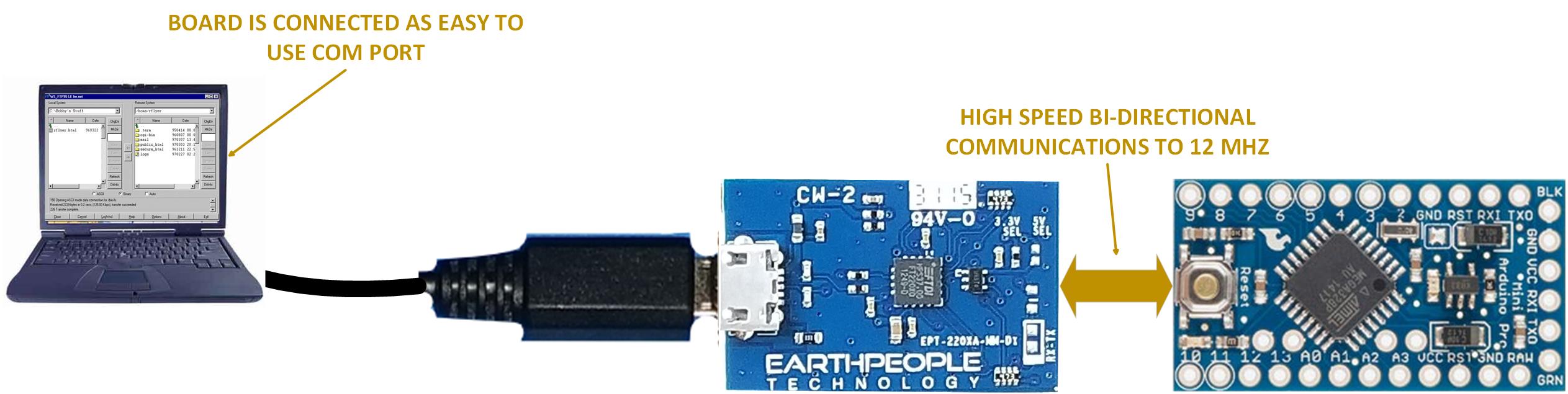
Hardware Features:
- USB 2.0 Full Speed
- Independent USB to SPI Slave Bus Running 12MHz Max Clock Speed
- Board is used as COM Port on the PC
- USB Powered
- Provides external +3.3volts @ 50mA
- FT220X FTDI chip has on chip 512 byte Receive and Transmit Buffers
- Compatible with any external +5/3.3 Volt MCU (Including all Arduinos)
Description
| The USB SPI Slave Breakout Board consists of the FT220X chip from FTDI. This single chip solution connects the Slave SPI bus directly to USB. The board includes a USB Micro B connector and two 1x8 0.1 inch headers. The board is powered from the USB port of the PC. It provides +3.3V regulated output to power up user MCU’s or any other power need. Current from the +3.3V regulated output is 50mA. No external power is needed for the USB SPI Slave Breakout Board. |

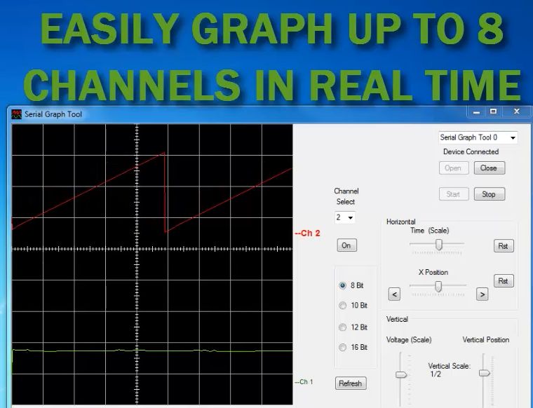
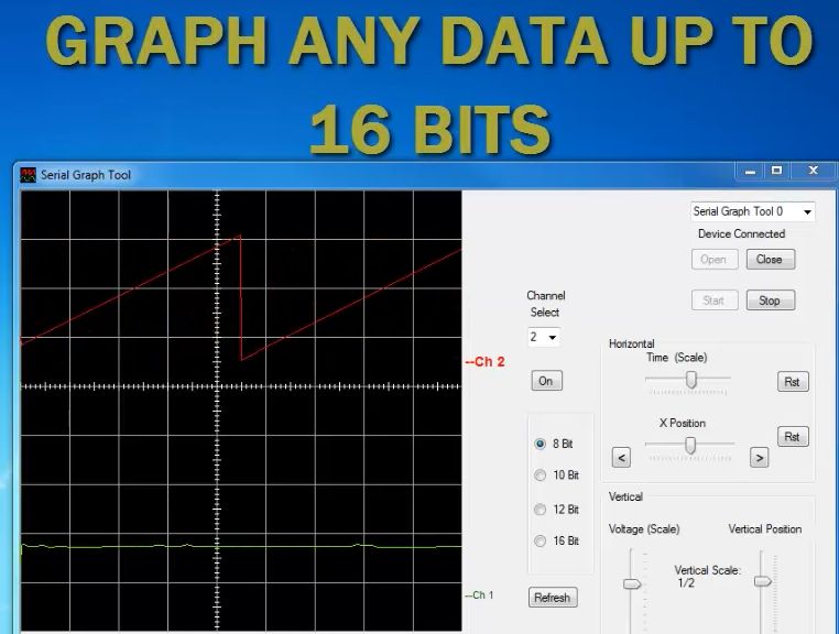
High Speed Data Display
| The USB SPI Slave Breakout Board comes with example software that displays data from the External MCU (Such as the Arduino Mini Pro). The user can display multiple channels of data analog, temperature sensor or digitally generated data. |
Downloads
| 85-000040 | USB SPI Slave Breakout Board User Manual | USB_SPI_SLAVE_BREAKOUT_BOARD_UM.pdf |
| 95-000040 | USB SPI Slave Breakout Board DataSheet | USB_SPI_SLAVE_BREAKOUT_BOARDL_DS.pdf |
| 45-000040 | USB SPI Slave Breakout Board Projects DVD | USB_SLAVE_SPI_BREAKOUT_PROJECT_3.0_DVD.ZIP |
| 55-000040 | USB SPI Slave Breakout Board Schematics | USB_SPI_SLAVE_BREAKOUT_SCHEMATICS.PDF |
| 35-000001 | EPT Drivers | EPT_2.12.00.exe |
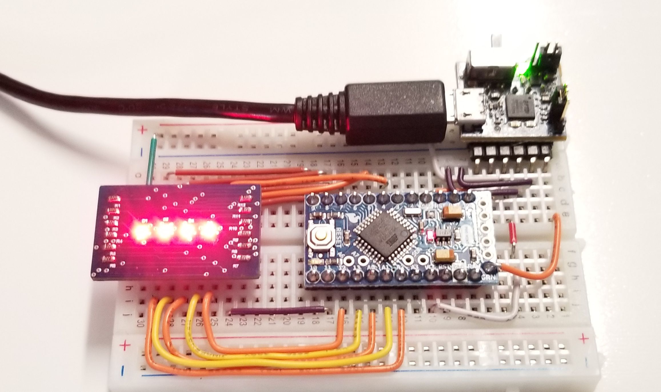
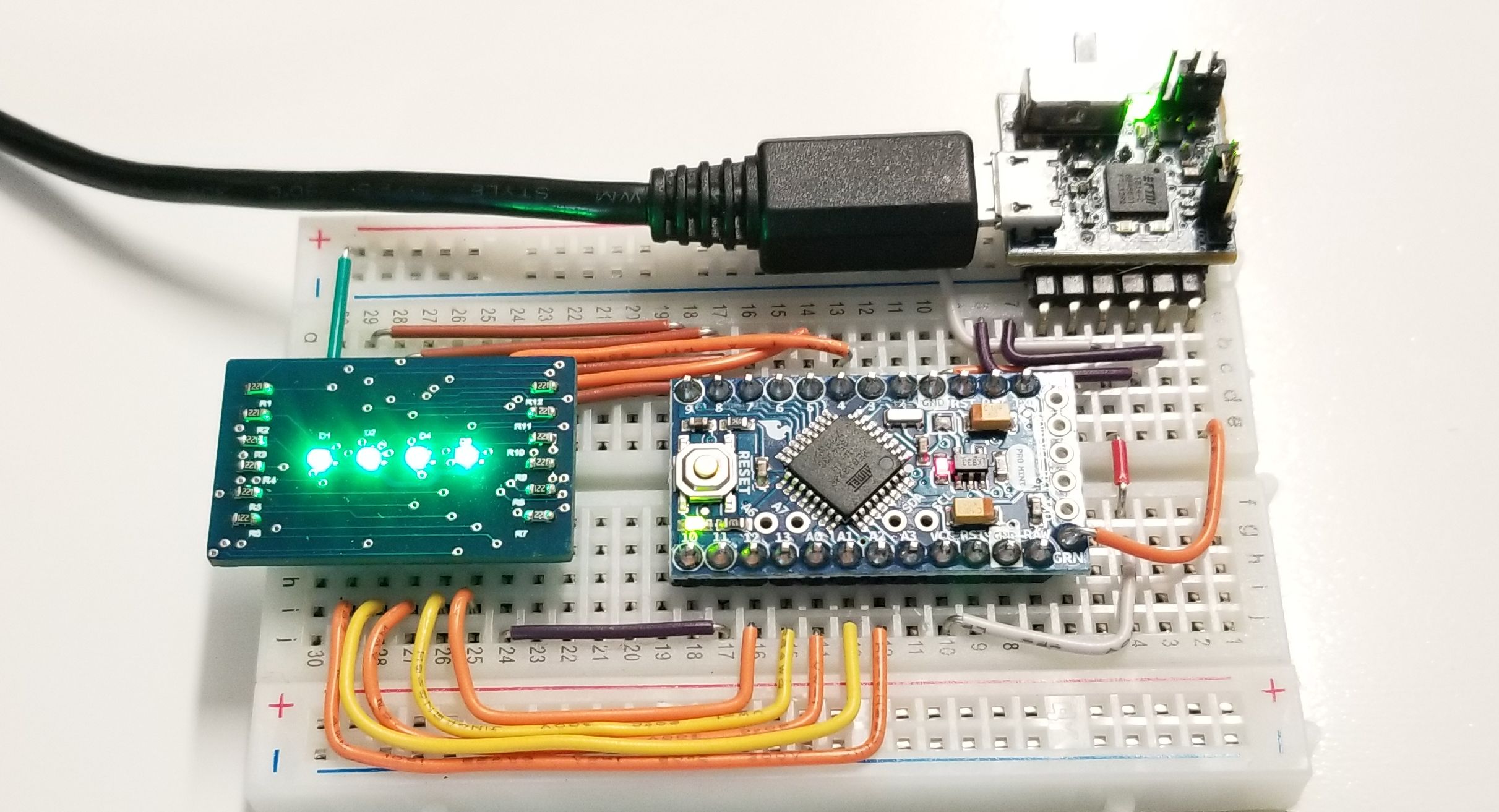
LED RGB Breakout Board
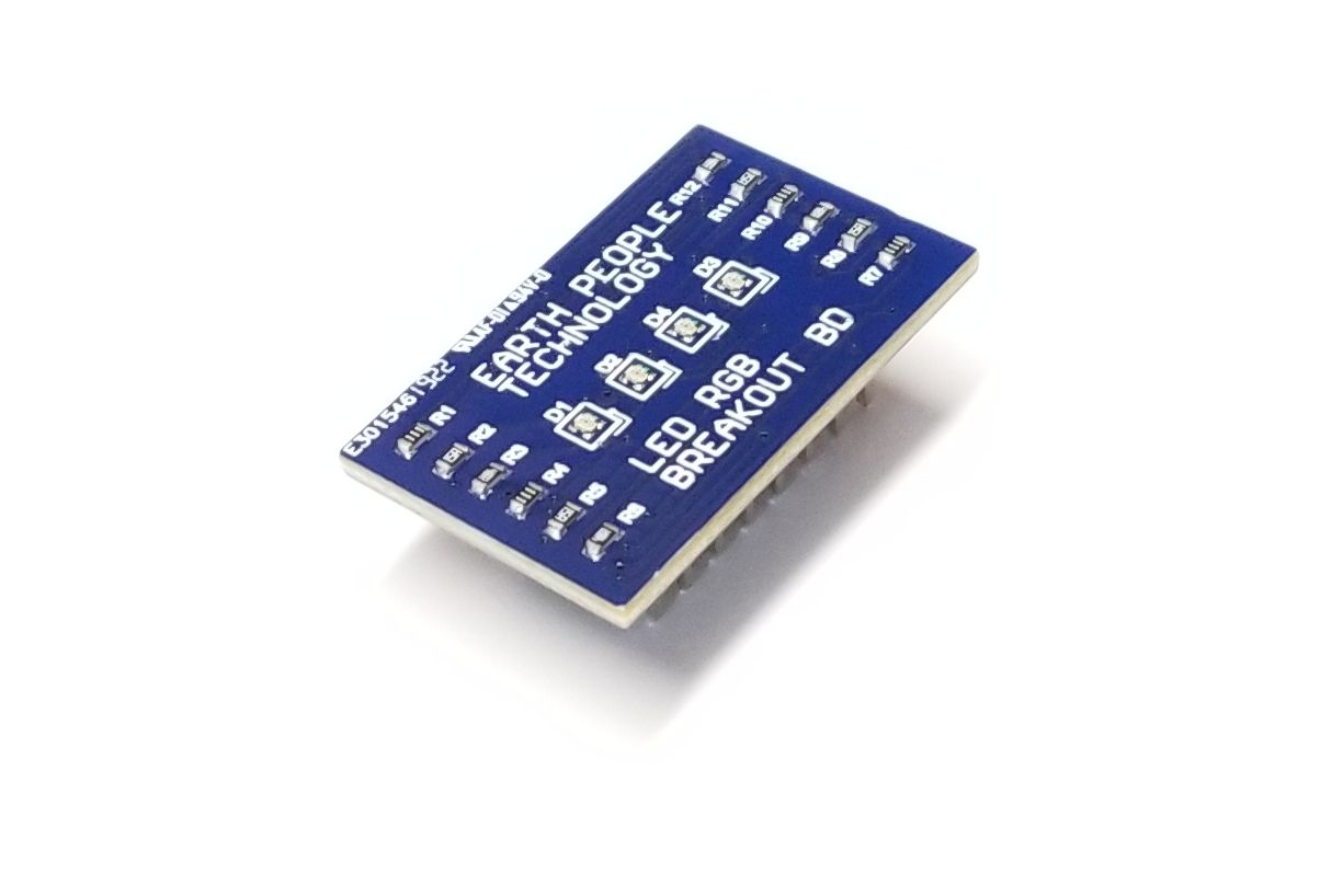

 LED RGB Breakout Board
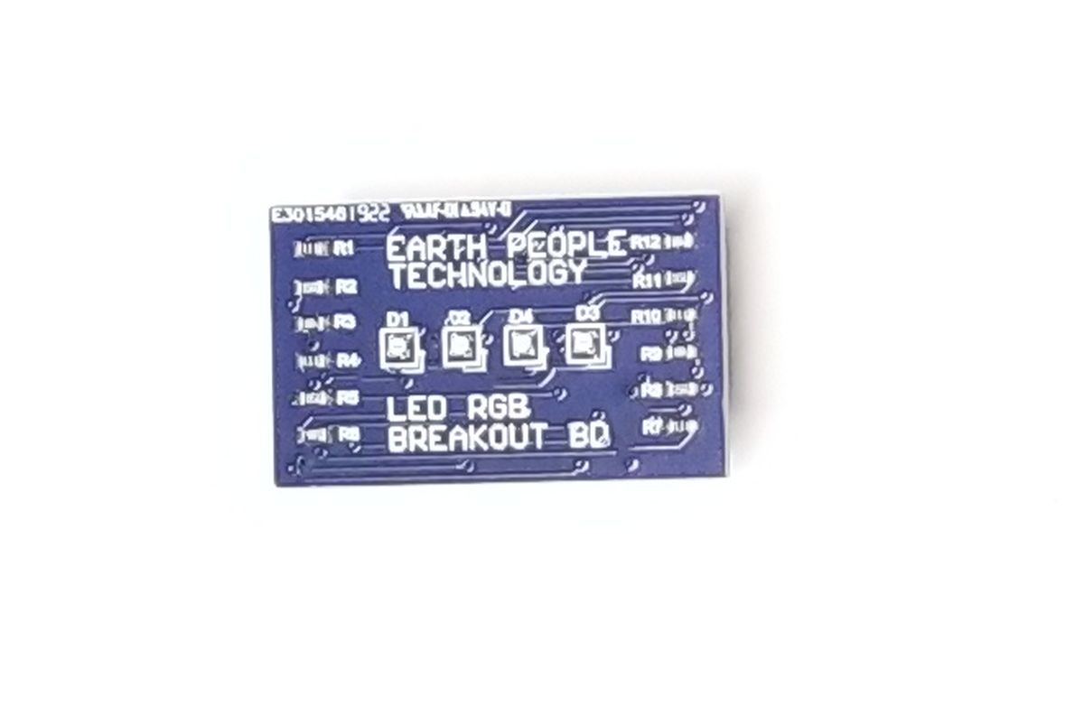
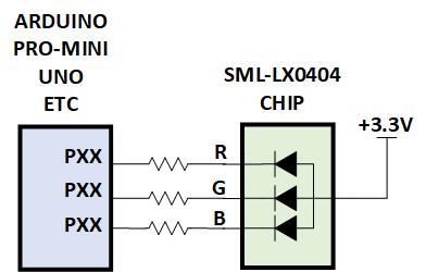
SML-LX0404 LED RGB Breakout BoardThe LED RGB Breakout Board provides a simple interface to control four LED RGBs for |
Hardware Features:
|
Description
| The LED RGB Breakout Board consists of four Lumex SML-LX0404SIUP LED chips. The SML-LX0404 chip is a current sink and can be connected to any MCU. The anode should be connected to +3.3V. The reason for this is the Series resistors are calculated for current limiting based on +3.3V. Changing the anode voltage to another source will change the brightness emitting from each LED. Because the SML-LX0404 chips are current sink, the user can connect to either +5V or +3.3V Arduino (or other MCUs) and control each LED. |
LED Electrical SpecificationsEach LED current limiting resistor is calculated to provide 5mA in each |
| Parameter | Red LED | Green LED | Blue LED | Units |
|---|---|---|---|---|
| Peak Wavelength | 632 | 518 | 564 | nm |
| Forward Voltage | 1.75 | 2.75 | 2.60 | Volts |
| Leg Current | 5 | 5 | 5 | mA |
| Resistor | 310 | 110 | 140 | Ohms |
| Axial Intensity | 30 | 40 | 20 | mcd |
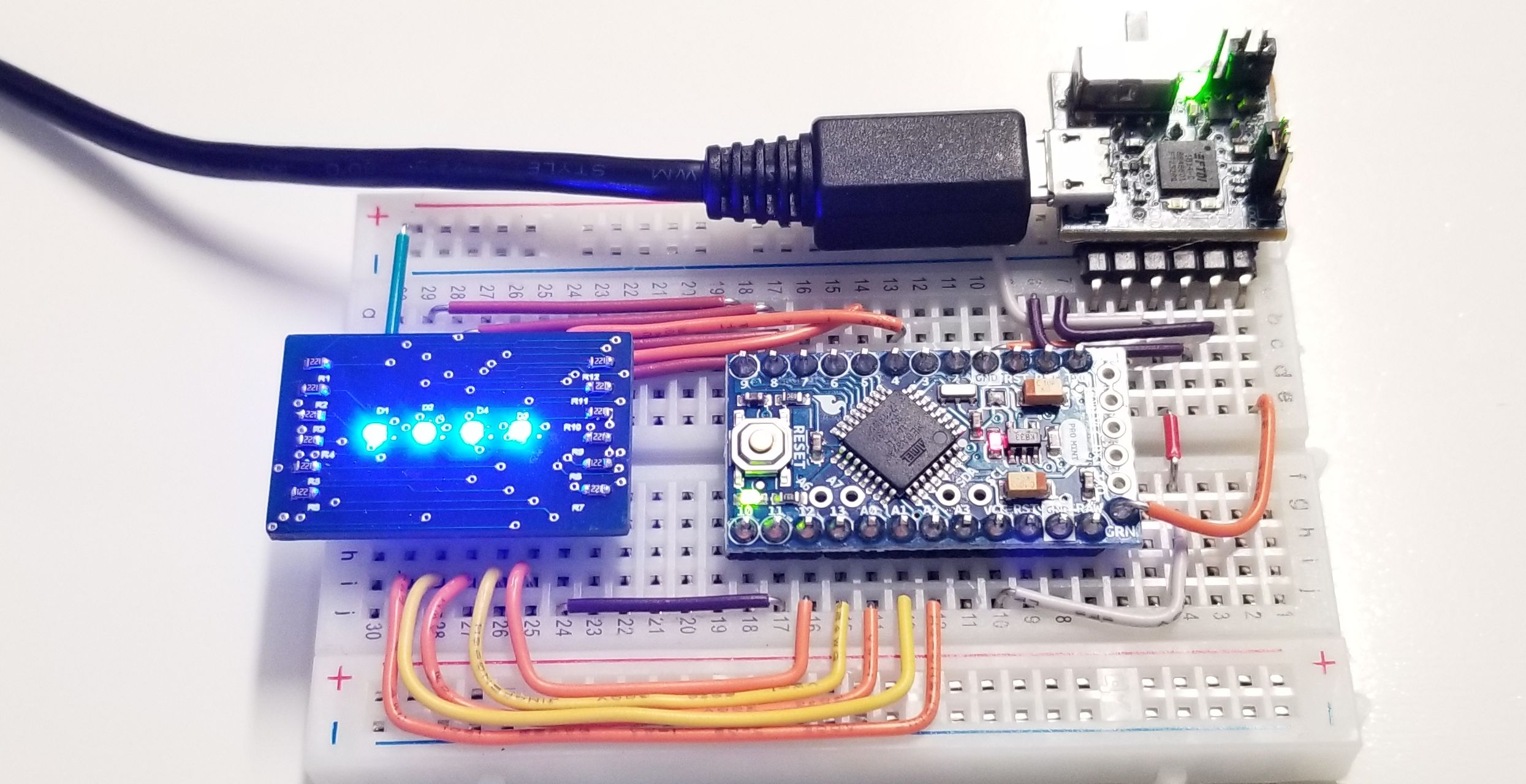
Earth People provides sample software so the user can use the Arduino functions
to control the LED RGBs. The user can control all aspects of each LEDs on/off time.
Adding pulse width controlled signals to the LEDs
allows a wide variety of colors to be displayed by the LED RGBs.
Easily Control four LED RGBs from an Arduino
| The LED RGB Breakout Board comes with example software that blinks individual LEDs from the External MCU (Such as the Arduino Mini Pro). The user can display multiple colors using each LED RGB. The MCU will provide pulse width modulated control for each LED. Changing the duty cycle of each LED changes the overall color of the LED RGB. |
Downloads
| 85-000040 | LED RGB Breakout Board User Manual | LED_RGB_BREAK_OUT_UM_V2.pdf |
| 95-000040 | LED RGB Breakout Board DataSheet | LED_RGB_BREAKOUT_BOARD_DS_V3.pdf |
| 45-000040 | LED RGB Breakout Board Projects DVD | LED_RGB_BREAKOUT_PROJECT_1.0_DVD.ZIP |
| 55-000040 | LED RGB Breakout Board Schematics | LEDRGBV1.3_Schemtic.pdf |
Seven Segment LED Board
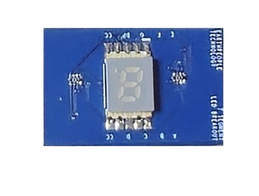
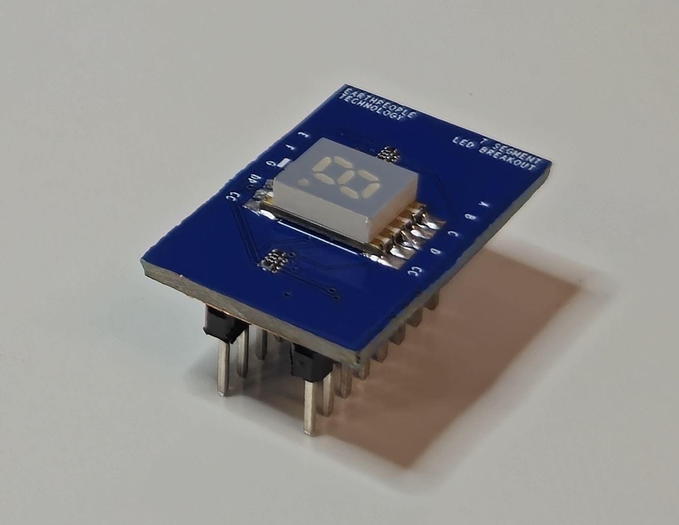
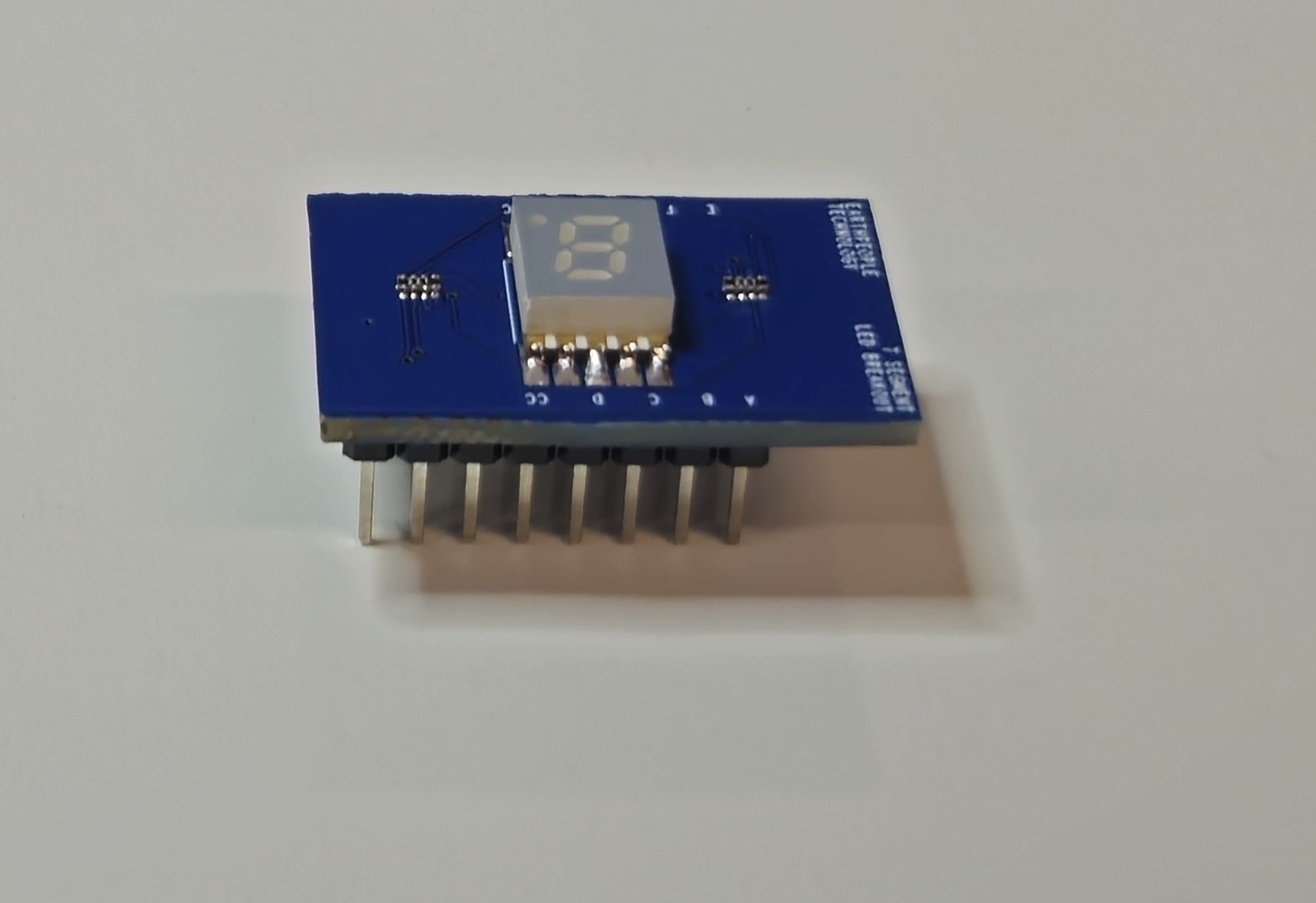 Seven Segment LED Board
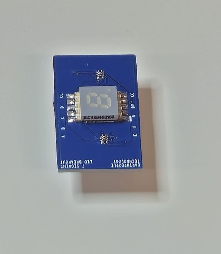
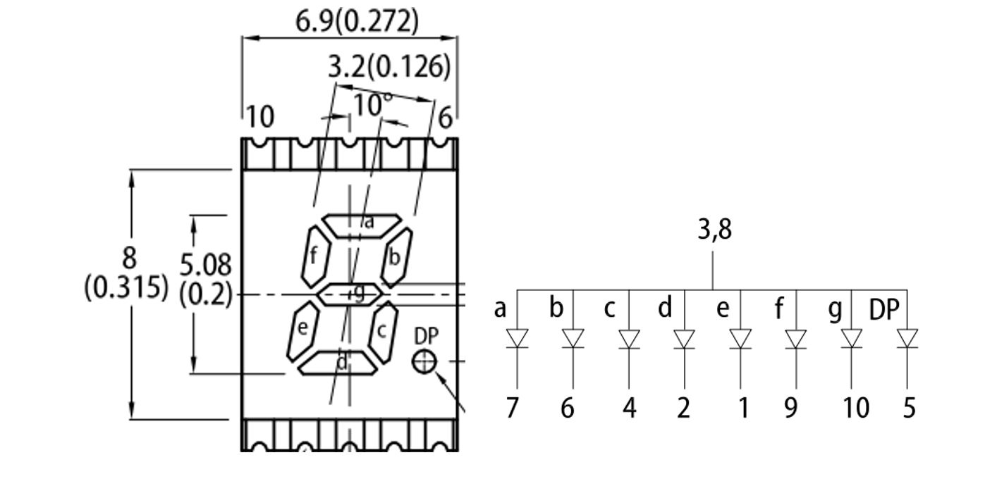
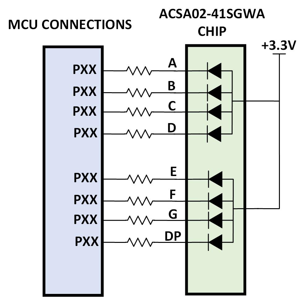
Seven Segment LED BoardThe EPT-ACSA02-LD-X2 is a breakout board that includes one Seven Segment LED. |
| The Seven Segment LED board uses one ACSA02-41SGWA-F01 manufactured by Kingbright. The Display is 0.2 inch digit height. It has low current operation and excellent character appearance. The Super Bright Green source color devices are made with Gallium Phosphide Green Light Emitting Diode. |
Hardware Features:
|
Description
| Each LED current limiting resistor is calculated to provide 5mA in each of the LED Segments. These current limiting resistors cannot be changed The ACSA02-41SGWA-F01 chip is a current sink and can be connected to any MCU. The anode should be connected to +3.3V. The reason for this is the Series resistors are calculated for current limiting based on +3.3V. Changing the anode voltage to another source will change the brightness emitting from each LED. Because the ACSA02-41SGWA-F01 chips are current sink, the user can connect to either +5V or +3.3V Arduino (or other MCUs) and control each LED. |
LED Electrical SpecificationsEach LED current limiting resistor is calculated to provide 5mA in each |
| Parameter | Symbol | Emitting Color | Value | Units |
|---|---|---|---|---|
| Peak Wavelength | Super Bright Green | 565 | nm | |
| Dominant Wavelength IF = 10mA | Super Bright Green | 568 | nm | |
| Spectral Bandwidth at 50% | Super Bright Green | 30 | nm | |
| Forward Voltage IF = 10mA | Super Bright Green | 2.0 | V | |
| Reverse Current (VR = 5V) | Super Bright Green | 10 | uA |
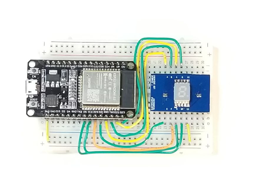
Easily Control Seven Segment LED Display from an Arduino
| The Seven Segment LED Board comes with example software that blinks individual LEDs from the External MCU (Such as the Arduino Mini Pro). The user can display characters using each LED Display. The MCU will provide pulse width modulated control for each LED. Changing the duty cycle of each LED changes the overall brightness of each segment of the LED Display. |
Downloads
| 85-000040 | Seven Segment LED Board User Manual | LED_SEVEN_SEGMENT_BOARD_UM_V1.pdf |
| 95-000040 | Seven Segment LED Board DataSheet | LED_SEVEN_SEGMENT_BOARD_DS_V2.pdf |
| 45-000040 | Seven Segment LED BoardProjects DVD | SEVEN_SEGMENT_LED_PROJECT_1.0_DVD.ZIP |
| 55-000040 | Seven Segment LED Board Schematics | LED_SEVEN_SEGMENT_SCHEMATIC_V1.pdf |
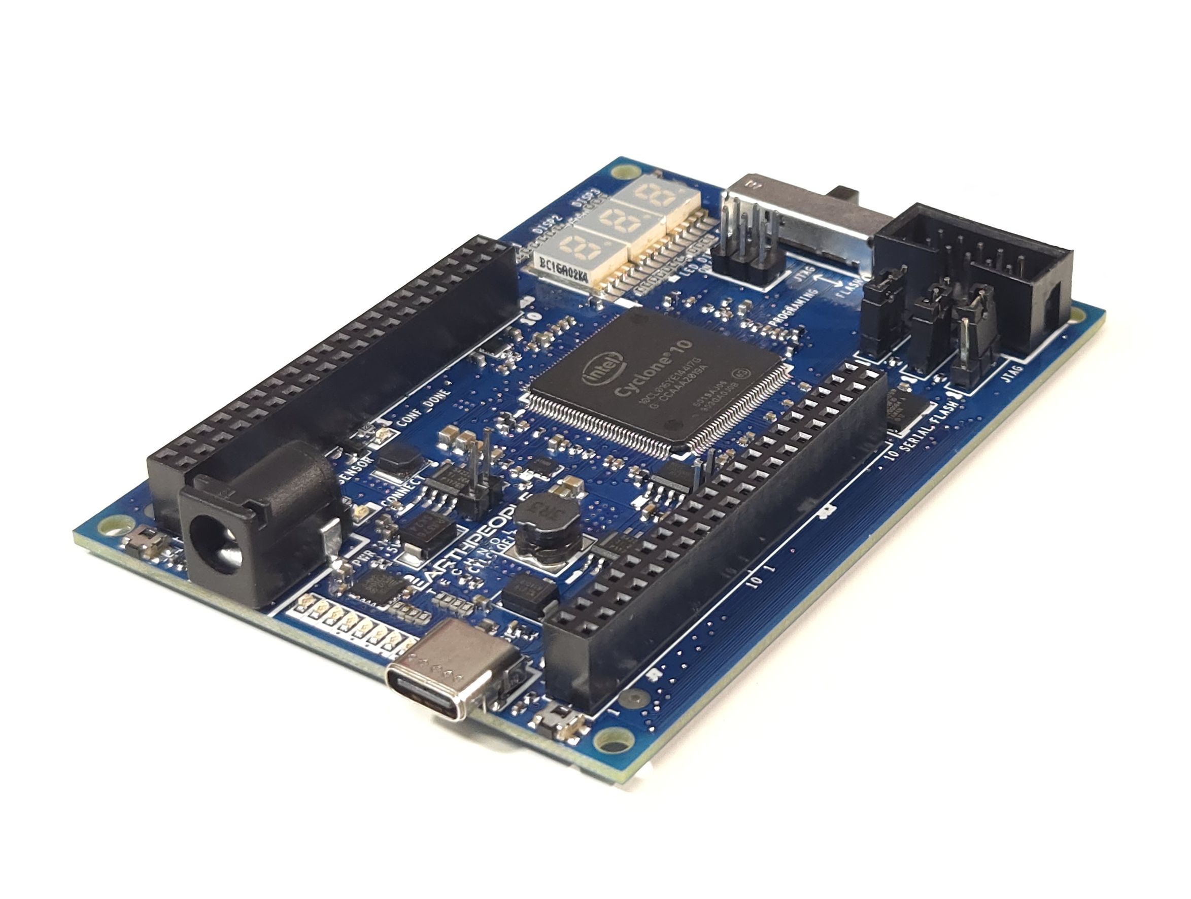
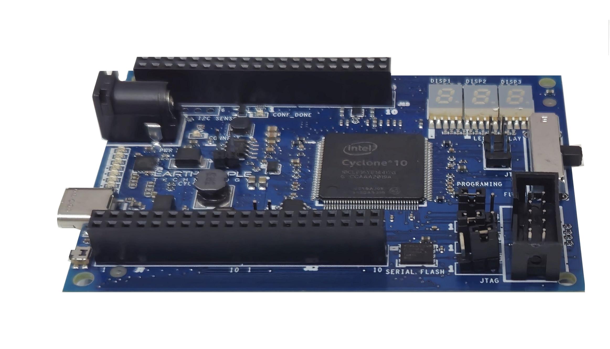
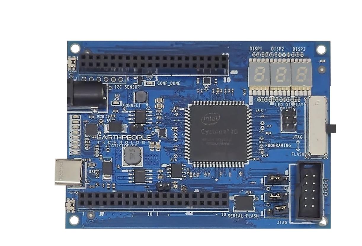
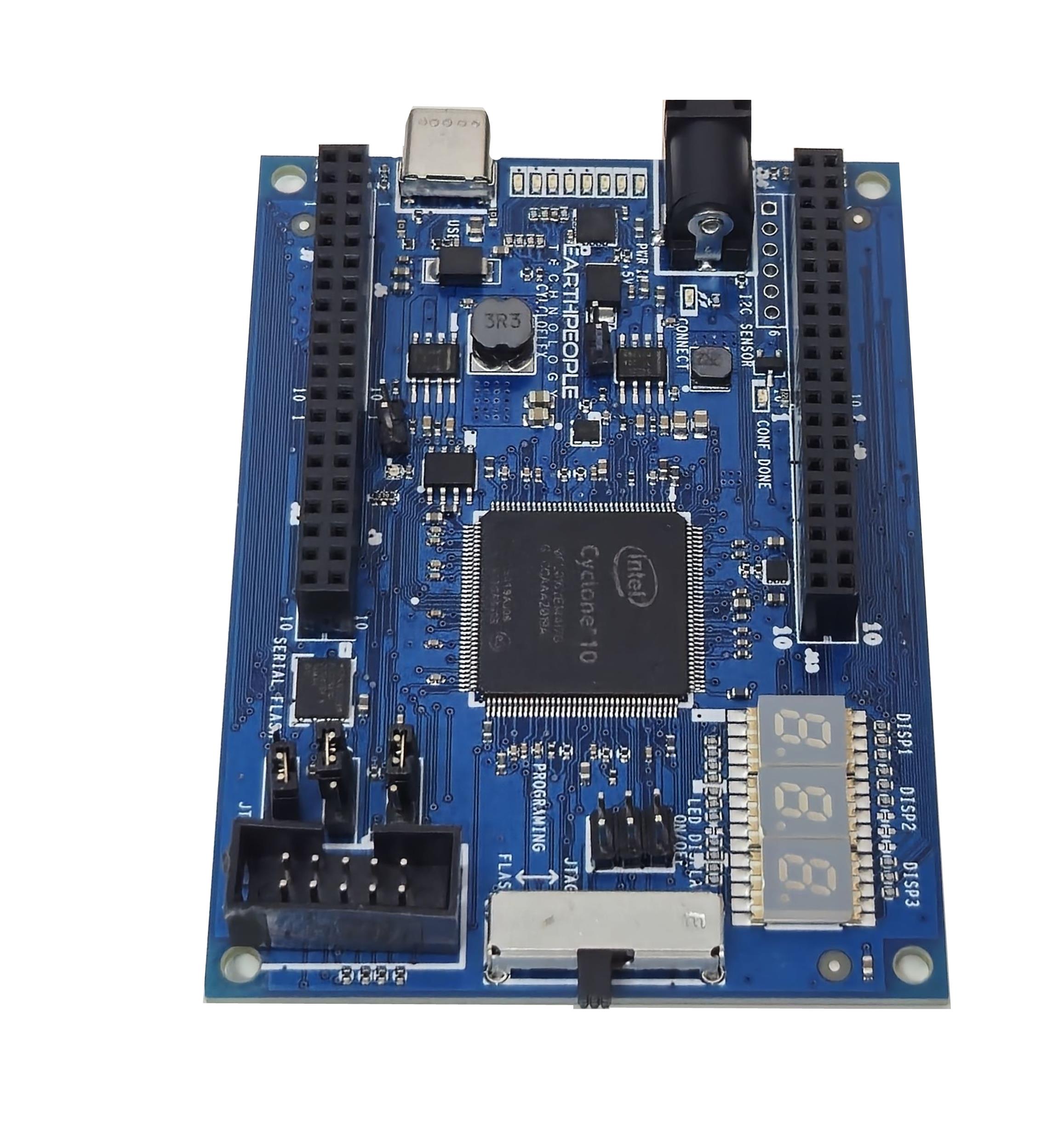
CycloFlex FPGA Development Board
CYCLOFLEX FPGA
DEVELOPMENT BOARD
The CycloFlex is an FPGA development board that is designed for the intermediate
user with some experience designing FPGA projects.
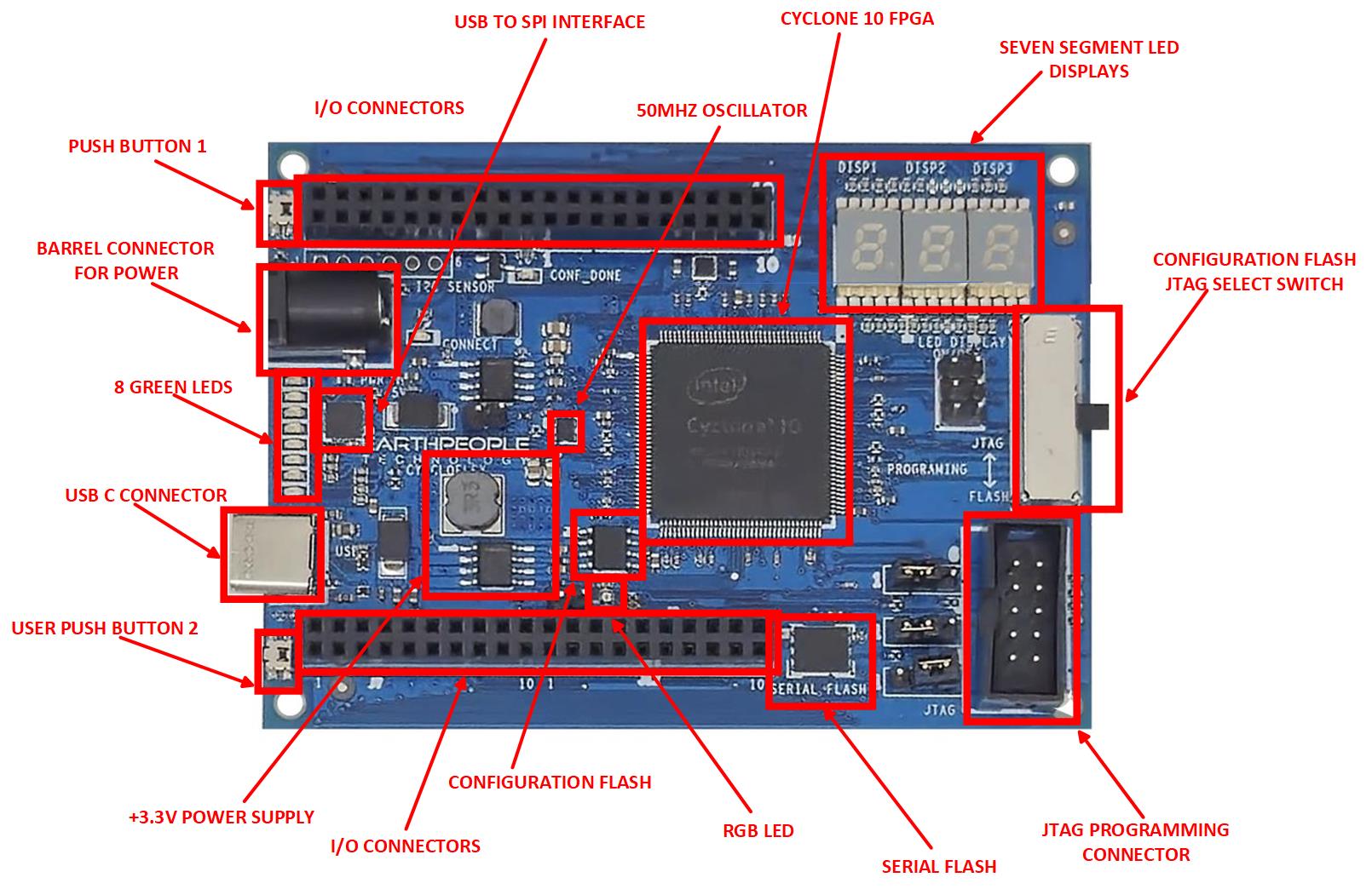
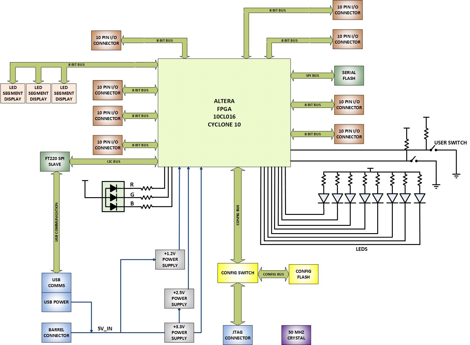
| The CycloFlex is packed with powerful features. The core of the CycloFlex is the Altera Cyclone 10 FPGA. This powerful chip has 16,000 Logic Elements and 504Kbits of Memory. The board includes a 128Mbit Serial Flash chip which allows the board to store up user code for using the FPGA as RISC V soft processor. There are three Green Seven Segment LED Displays, RGB LED and Eight User LEDs. It allows the creation of more diverse projects than beginner projects. |
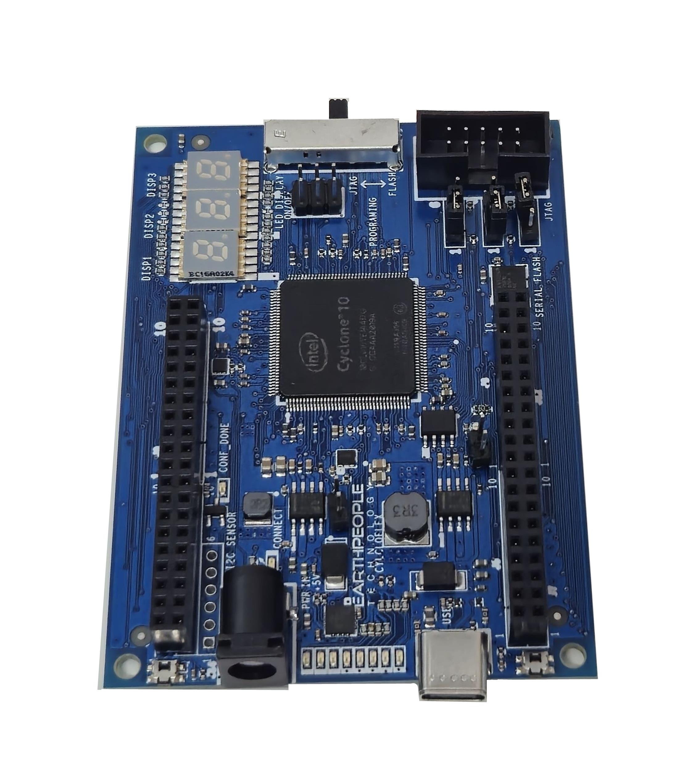
Please Note: The CycloFlex Does Not Contain On Board Programmer.
JTAG Programming and Configuration Flash Programming must be
performed by external Programmer Purchased Separately.
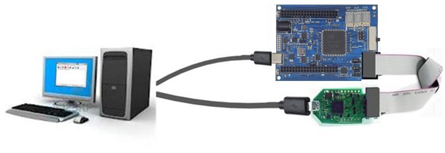
| This board provides a powerful platform for developing and debugging programmable logic code. It has been designed from the ground up to provide the functionality needed for the demanding projects from todays students and hobbyists. The board provides a convenient, user-friendly work flow by connecting seamlessly with Altera’s Quartus Prime Lite software. The user will develop the code in the Quartus environment on a Windows Personal Computer. The programmable logic code is loaded into the FPGA using only the Quartus Programmer tool. |
CycloFlex FPGA Development Board
|
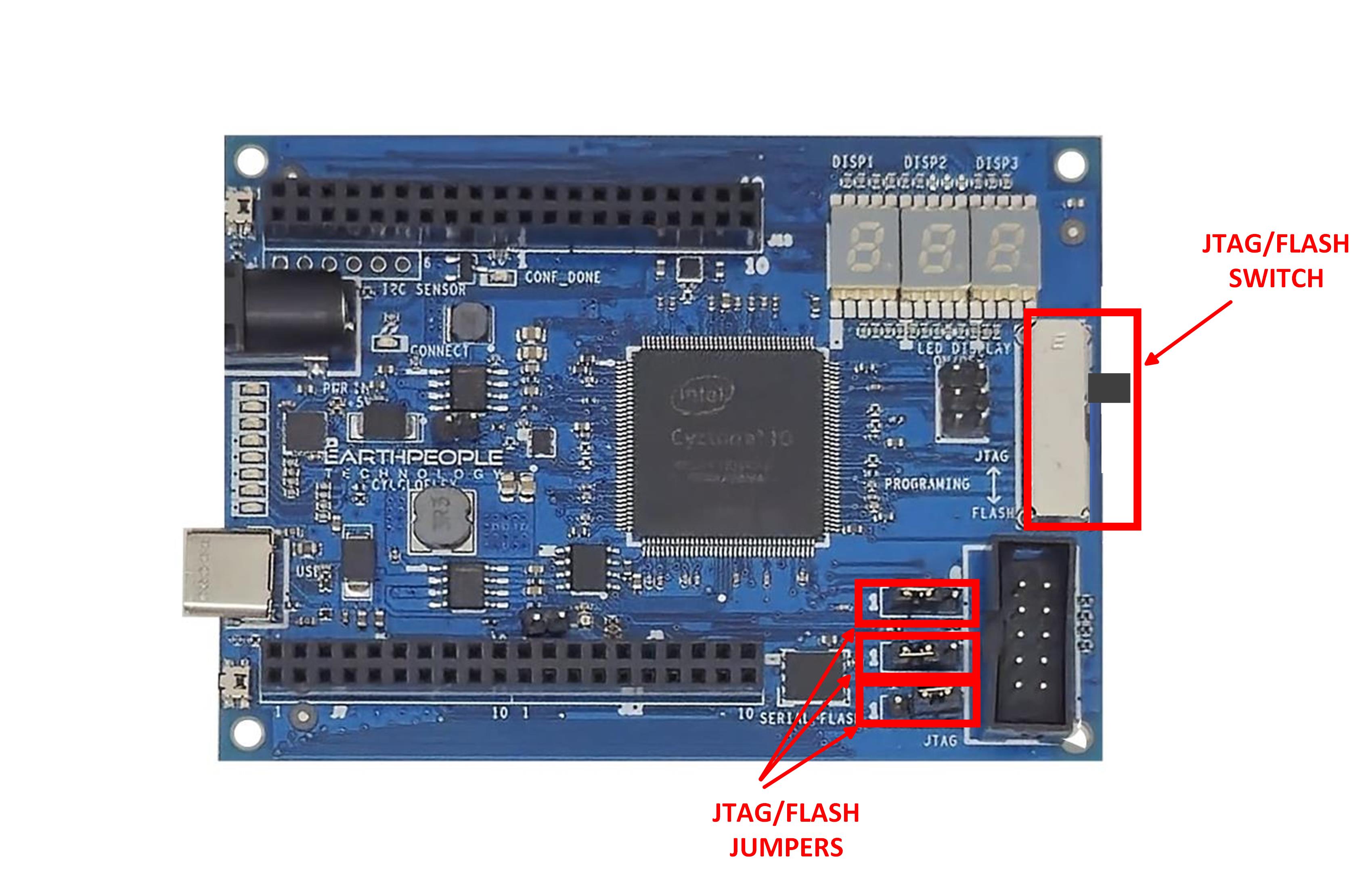
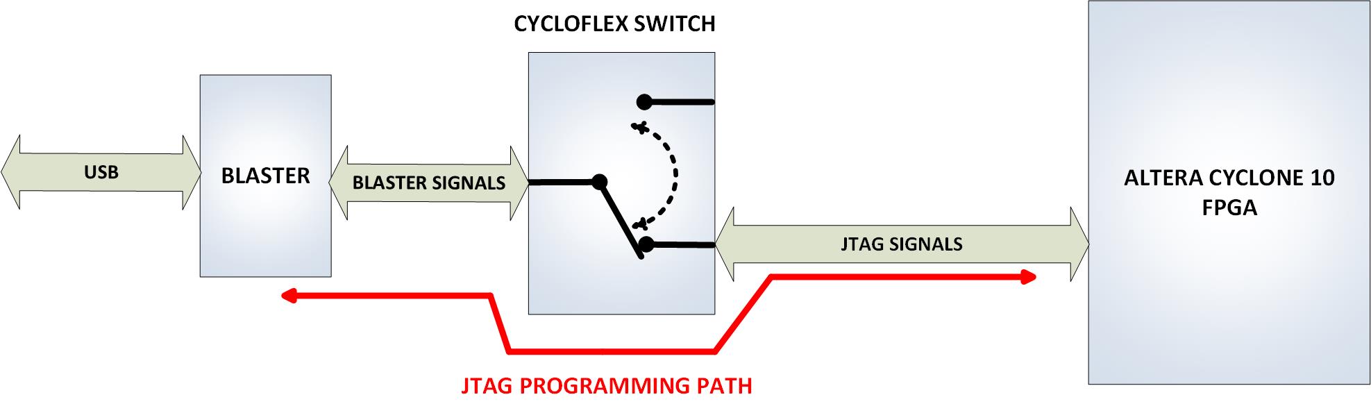
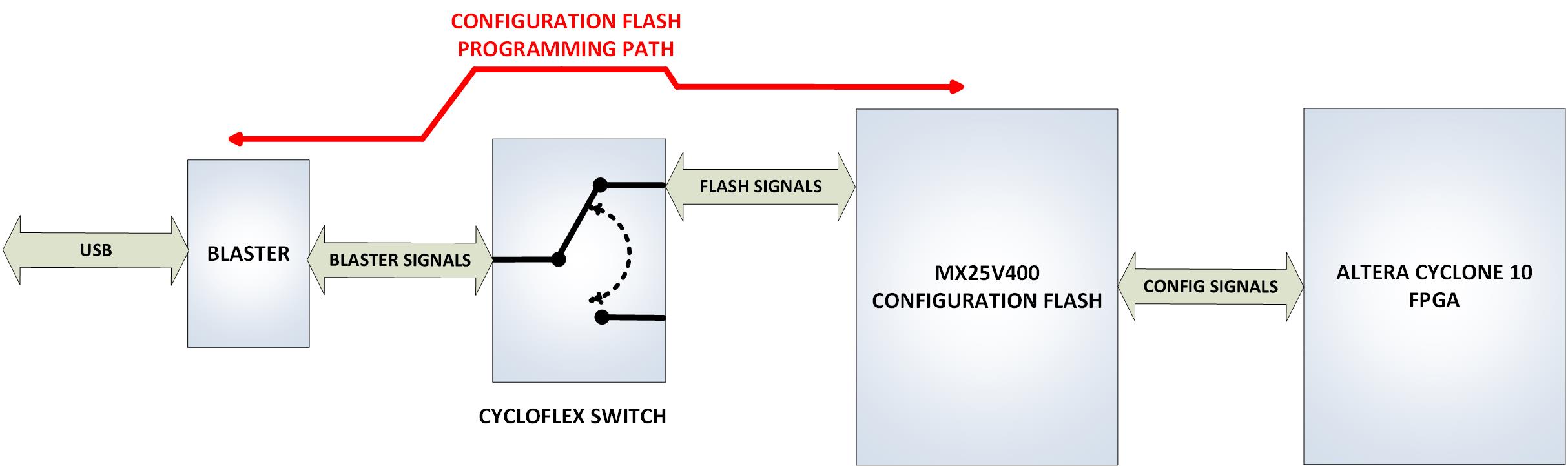
Two Programming Options on the CycloFlex
|
The CycloFlex allows the user to choose between Direct JTAG programming using the *.sof file and programming the configuration Flash with a flick of a switch.
Configuring the Cyclone 10 FPGA on the CycloFlex is the process of
Direct JTAG access allows the Quartus Prime Lite software to program the
The Cyclone 10 FPGA requires configuration before it can be used to perform
|
CycloFlex Communications
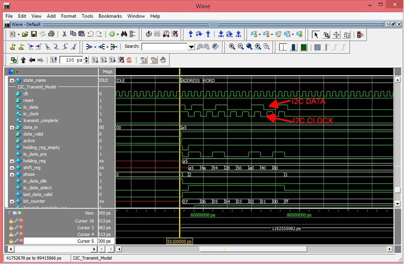
| The CycloFlex has an on board USB to SPI Serial FTDI chip to connect directly to the FPGA. This chip is the FT220X chip which allows a Host PC to communicate with the FPGA. The FT220X chip provides all of the USB protocol and is transparent to the user. The Input/Output side of the chip provides a modified version of the accepted SPI bus. It uses FTDI’s proprietary FT1248 protocol.
Earth People Technology has created demonstration software that provides a |

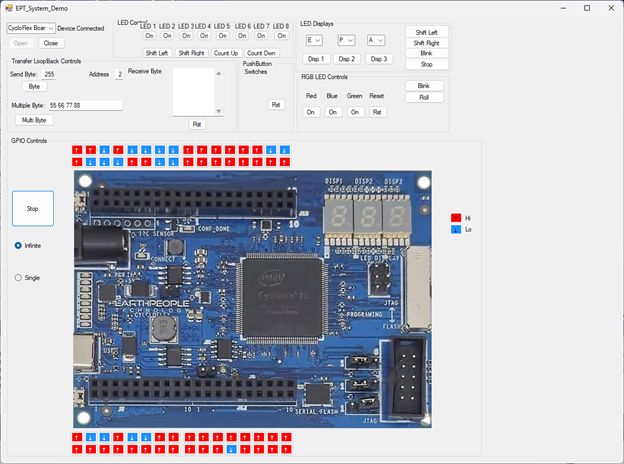
Pre-Loaded With System Demo Software
The CycloFlex board comes pre-loaded with the EPT_System_Demo HDL project in the
FPGA. This project allows the user to test out the functions of the Active Host API
and the board hardware. The software is a multi-function Test Tool which allows the
user to turn On/Off the RGB LEDs, Change the speed/control of the User LEDs, display
characters on the Seven Segment LEDs, test the Push Button Switches and Send/Receive
Bytes from the FPGA. The System Demo Software also has a "Poor Mans Logic Analyzer"
which displays the current status of the Inputs/Outputs at the connectors.
This software demonstrates the USB to SPI communications with the FPGA as well as the
EPT API Active Host Library. All source code and compiled projects are included on the
DVD for the user.
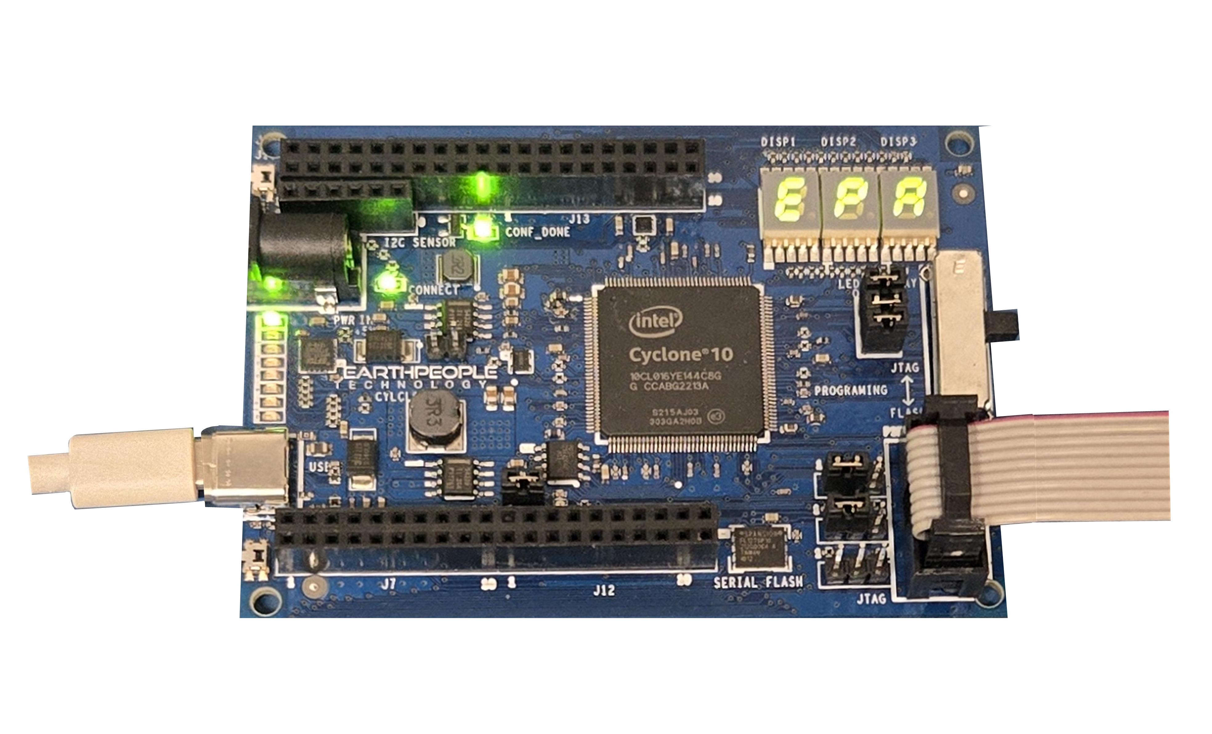
THE CYCLOFLEX HARDWARE
| The CycloFlex is Hardware based on the Cyclone 10 FPGA. The board has 64 Inputs and Outputs connected to 0.1 Inch Headers at the board edge. These are organized as eight 10 pin connectors to allow users to connect to off board circuits. Some of the headers contain +3.3VDC and Ground connections.
The CycloFlex contains three Seven Segment LED Displays. These displays are
The CycloFlex has a Serial Flash chip on the bottom right board. This allows |
THE CYCLOFLEX AND SIMULATION
| Simulation has always been a weak point for students and hobbyists. Most FPGA beginners write the user code, compile it, synthesize it, program the chip then test out the results. While this approach may work for small, simple designs, it quickly becomes a problem with larger projects. As the user code increases in complexity, better development tools are required to quickly isolate problems. The premier method for this is functional testing.
ModelSim/Questa is included Free with the Quartus Prime Package. ModelSim/Questa is a |
|
| In short, the CycloFlex will cut the time to get the time to get up and running significantly. We also include several pre-made, fully compiled, fully synthesized projects for the user. You can start your project by copying one of these premade projects and adding user code. |
Downloads
| 85-000113 | CycloFlex FPGA Development System User Manual | CYC_MAX_FPGA_DEV_SYS_UM.pdf |
| 95-000113 | MaxProLogic FPGA Development System Data Sheet | CYCLOFLEX_FPGA_DEV_SYS_DS.pdf |
| 45-000113 | CycloFlex FPGA Development System Project DVD | CYCLOFLEX FPGA PROJECT DVD |
| 55-000113 | CycloFlex FPGA Development System Schematics | CYCLOFLEX SCHEMATICS.pdf |
| 35-000100 | EPT Drivers | CDM212365_SETUP.ZIP |
JTAG Blaster II

 JTAG Blaster II
JTAG Blaster II Provides JTAG connectivity for Altera FPGAs, CPLDs and Flash devices only |
|
The JTAG Blaster II is a USB Based Programmer Adapter specifically designed to program Altera’s FPGA’s, CPLD’s and Flash chips. The board is a stand alone, USB powered device that can program Altera’s devices using +1.8V to +5.0V. It uses a USB-C cable to connect to the Host. And a 10 pin connector to connect to the device to program. |
Program CPLDs and FPGAs
|
The JTAG Blaster II is designed as a direct replacement for the original USB Blaster from Altera. The board programs Altera FPGA’s, CPLD’s and Flash chips at the default speed of 6MHz. It uses the driver included with the Quartus Software. So, there is no external software to install to get the JTAG Blaster II working. Just plug the USB-C cable into a laptop with Quartus and connect to the board. The Quartus Software will automatically recognize the JTAG Blaster II as a USB Blaster. |
Specifications
Features:
|
Supported Software:
|
Supported Devices:
|
JTAG Blaster Connection and Programming LEDs
|
The board includes a “CONNECT” LED. This LED will light Green once the board has been fully enumerated by the Host PC. Enumeration happens because the FT245 USB to Parallel chip has been properly powered by the on board supply and the Host PC recognizes the board and the Host PC has successfully loaded the appropriate driver for the board.
The JTAG Blaster II includes an RGB LED in the lower right corner
This LED will light up Blue when the programming is idle. When |


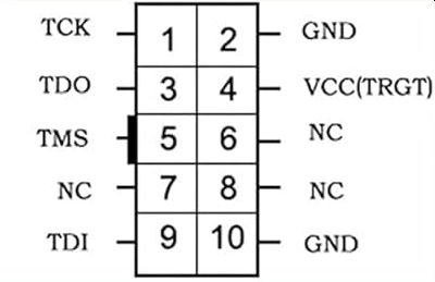
JTAG Connector
|
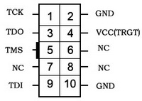
The JTAG Blaster includes a 5x2 Shrouded Male Header that comprises the JTAG Connector to connect to target device. Pin 1 located in the upper left corner.
The pinout of this connector is the standard Altera pinout.
Altera Standard PS Signals Pinout The JTAG Connector utilizes the standard pinout of the Altera USB Blaster.
In this case, we connect to the MaxProLogic using the 10 pin Ribbon cable. |


No Driver Needed
|
The JTAG Blaster II uses the Driver from the Quartus Prime Software. There is no external or third party driver needed. Just connect the JTAG Blaster to an available USB port on a PC with Quartus Installed
And the Quartus Prime Software will automatically recognize the JTAG |


Downloads
| 85-000012 | EPT JTAG Blaster II User Manual | EPT_JTAG_BLASTER_II_UM_V3.pdf |
| 95-000013 | EPT JTAG Blaster II Data Sheet | EPT_JTAG_BLASTER_II_DS_V2.pdf |
| 45-000013 | EPT JTAG Blaster II Project DVD | JTAG_BLASTER_II_PROJECT_1.0_DVD.zip |